For decades, the trajectory of the global IT industry has been governed by a single empirical rule—a principle that evolved into the secular canon of the digital era. Moore’s Law transcended its origins as a mere observation to become an economic metronome, dictating the cadence of investment, R&D, and the expectations of millions. Today, however, the physical limitations of silicon and the mounting inertia of software are jeopardizing this long-standing paradigm. To avert technological stagnation, the industry is charting new courses, diversifying its survival strategy across three fundamentally distinct vectors.
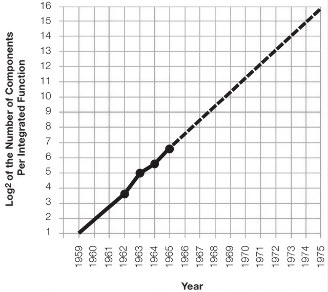
The saga of Moore's Law traces back to 1965, when Gordon Moore, co-founder of Intel, observed a compelling pattern: the number of transistors on integrated circuits doubled with a predictable regularity. Initially, this cycle spanned a single year, later extending to two, and by the early 2000s, it evolved into a benchmark for performance growth every 18 months. While never a law of physics in the strictest sense, it became a self-fulfilling prophecy. Engineers worldwide raced to keep pace with this trajectory, fearing that any deviation would leave them on the periphery of progress.
By 2015, Moore himself warned that infinite scaling was an impossibility. By 2026, this forecast had effectively materialized: the industry hit a physical wall where classical miniaturization methods simply cease to function. Nevertheless, attempts to "resuscitate" Moore's Law persist, as it remains the bedrock for long-term strategic business planning.
The enduring relevance of this rule was rooted in economics. The cost of a microchip was inversely proportional to its component density: the more transistors that could be packed onto a die, the lower the cost per unit of computing power. This created a virtuous cycle—manufacturers slashed overhead while customers gained increasingly powerful systems, accelerating the return on investment.
However, this triumph of hardware birthed an unforeseen side effect in software development. Relying on the guaranteed surge in processor power, programmers began to neglect code optimization. This gave rise to "Wirth's Law" (sometimes associated with Gates), which posits that software slows down faster than hardware speeds up. The burgeoning complexity of frameworks and high-level languages effectively "consumed" the dividends provided by Moore's Law. Paradoxically, it was this very abundance of resources that allowed modern machine learning and artificial intelligence—which demand colossal computational power—to flourish.
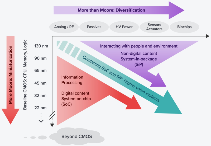
As transistor gate sizes approached the critical threshold of 25nm, the industry bifurcated its efforts into three distinct strategies: More Moore, More than Moore, and Beyond Moore.
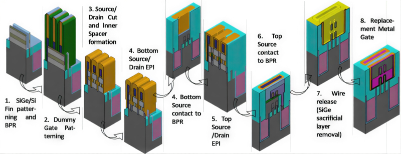
The first path, More Moore, represents the extensive evolution of current CMOS technologies. It is an attempt to extract every possible drop of performance from silicon through sophisticated engineering ingenuity. Rather than simply shrinking the footprint of elements, engineers are redesigning the transistor's very structure. The transition from FinFET to RibbonFET (Gate-All-Around) architecture allows the gate to literally "wrap around" the channel on all sides, radically reducing current leakage caused by quantum tunneling.
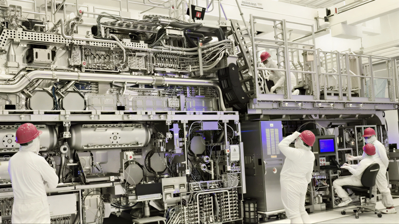
Further innovations, such as PowerVia and PowerDirect, move power delivery to the backside of the wafer. This mitigates parasitic interference and enables denser transistor packing. Meanwhile, the deployment of High-NA EUV lithography is pushing geometric scaling toward its absolute physical limit. This remains the most attractive path, as it leverages an existing multi-billion-dollar manufacturing infrastructure.

The second vector, More than Moore, proposes a paradigm shift from the monolithic die to modular systems. Instead of attempting to cram everything into a single giant chip, the industry is pivoting toward "chiplets"—specialized functional blocks linked by high-speed interconnects (such as Intel's Foveros or TSMC's CoWoS).
This approach allows for the combination of components manufactured using different process nodes. Not every block in a system requires cutting-edge 2nm precision; many tasks are handled efficiently by older, more cost-effective fabs. This not only reduces costs but also paves the way for cyber-physical systems. Integrating analog sensors and converters directly into a composite chip is critical for autonomous vehicles, neural interfaces, and the Industrial Internet of Things (IIoT), where digital logic must be seamlessly "stitched" to the physical world.
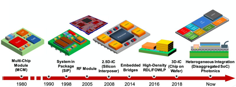
The third path, Beyond Moore, is a radical departure from the past—a rejection of semiconductors as we know them. This domain explores technologies that could entirely replace silicon. Photonics proposes using photons instead of electrons; while optical components are larger than transistors, the theoretical limit of computational intensity within a given space is incomparably higher.
Spintronics, which leverages electron spin, and neuromorphic computing, which mimics the architecture of the human brain, promise a fundamentally different level of energy efficiency. Quantum computing opens the door to classes of problems that were previously unsolvable for classical systems. This transition will likely necessitate the abandonment of the von Neumann architecture—which has dominated for decades—by collapsing the divide between memory and processor.
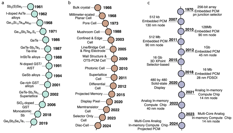
Today, the world stands on the threshold of a new era. Moore's old "metronome" can no longer set the tempo, but the demand for predictable progress remains. The industry is now striving to define a new roadmap, for without a clear vector of development, the cost of innovation could become prohibitively high, even for the world's largest corporations and sovereign states.
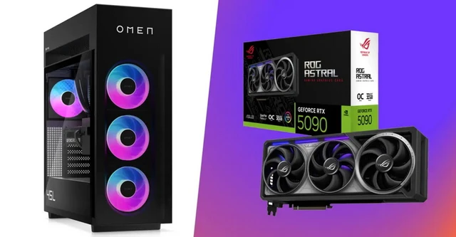 The Economic Paradox of the GeForce RTX 5090