The pursuit of smaller nanometer nodes has reached a critical juncture where conventional lithography is no longer economically or technically viable. Intel is doubling down on High-NA EUV—the most costly and precise patterning system in the history of semiconductor manufacturing. Crossing the threshold of one million processed wafers signals the transition of this technology from an experimental phase to full-scale industrial deployment. This milestone establishes a new industry hierarchy, distinguishing leaders by their readiness to radically overhaul their manufacturing stacks.
Modern semiconductor manufacturing is confronting a fundamental challenge: the physical resolution limits of existing lithography systems. The transition to High Numerical Aperture Extreme Ultraviolet (High-NA EUV) lithography is designed to overcome this bottleneck, enabling the printing of denser, more complex structures without the need for the cumbersome multi-patterning of a single layer. By becoming the first company to integrate this tool into an active production cycle, Intel is effectively rewriting the playbook for the semiconductor industry.
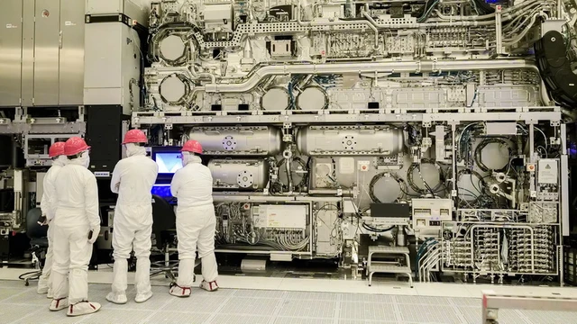
Initially, the ASML TWINSCAN EXE:5000 systems were earmarked for research and the debugging of the 14A process node. However, practical application has demonstrated that the potential of High-NA extends far beyond a single node. Intel has successfully integrated these tools into its 18A production, optimizing the fabrication of the Panther Lake processor family. Rather than relying on traditional Low-NA systems, the company is utilizing High-NA to manage the overlay of multiple silicon layers, significantly enhancing element positioning precision.
This technological breakthrough is evident not only in transistor density but also in the radical simplification of the manufacturing cycle. The deployment of the TWINSCAN EXE:5200B scanner has reduced the number of processing steps for a single layer from forty to fewer than ten. This reduction is critical: fewer steps translate to fewer opportunities for defects and a substantially shorter production cycle. Consequently, the throughput of Intel Foundry facilities has surged, reaching rates exceeding 30,000 wafers per quarter.
However, technological leadership comes at a staggering cost. A single High-NA EUV system from ASML costs approximately $400 million—nearly double the price of previous generation EUV scanners. Such extreme capital intensity creates a formidable barrier to entry, forcing competitors to seek alternative pathways.
Currently, the market is witnessing a clear divergence in strategies. TSMC is maintaining a conservative approach, seeking to extract maximum value from existing Low-NA systems through incremental optimization and process shrinkage. Samsung, according to available data, does not plan a full-scale transition to High-NA until 2030, synchronizing the move with the launch of its 1-nanometer process.
In effect, Intel has secured a strategic technological window of opportunity. While the rest of the industry focuses on optimizing legacy equipment, Intel is already scaling production based on High-NA and offering this configuration to external clients. This transforms the company from a mere chipmaker into the primary operator of the world's most advanced lithography stack—a factor that could prove decisive in the battle for dominance in the Foundry market.
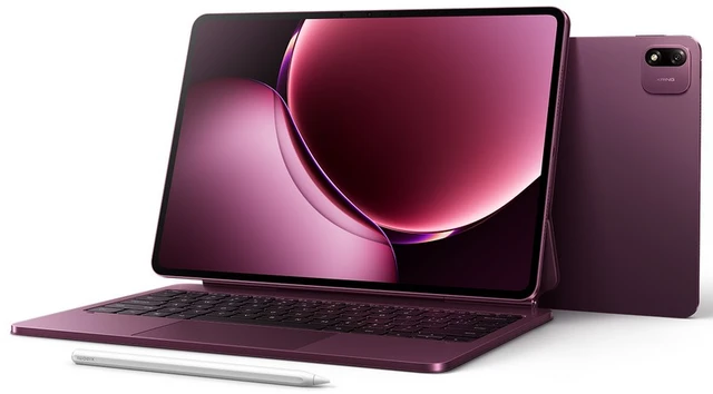 Power and Poise: The Xiaomi Pad 9 Pro Max