The global surge in demand for artificial intelligence and high-performance computing (HPC) is pushing memory manufacturers toward critical physical limits. In this high-stakes race, the transition to 10-nanometer-class process nodes has emerged as the primary battleground for technological supremacy. South Korean titan SK hynix is spearheading an aggressive migration of its production capacity to the 1c node, aiming to secure a decisive strategic advantage. This strategic pivot does more than just optimize data density; it lays the groundwork for the next generation of ultra-high-speed memory.
The DRAM industry is currently navigating a period of profound transformation, where the battle is fought over every nanometer and every lithographic layer. SK hynix is systematically transitioning its production capacities to the cutting-edge 1c process—the sixth generation of the 10nm-class node. The pace of this migration is striking: while the 1c share stood at a modest 10% in the first quarter of 2026, it is projected to exceed one-third of total production by year-end. By early 2027, the 1c node is expected to become dominant, accounting for approximately 35% of capacity, while the preceding 1b generation will hold 33%.
Crucially, process terminology in DRAM manufacturing diverges significantly from the standards used in logic chips for CPUs. When the industry refers to a "10nm-class" node, it is not describing the physical size of the transistor, but rather a collective set of scaling methodologies. In the case of SK hynix, the transition from the 1b node to 1c represents a physical reduction in element size from 12–13nm down to 11–12nm. The primary catalyst here is Extreme Ultraviolet (EUV) lithography. While the 1b process utilized four EUV layers, 1c increases this to five or six, enabling an extraordinary component density while maintaining signal stability.
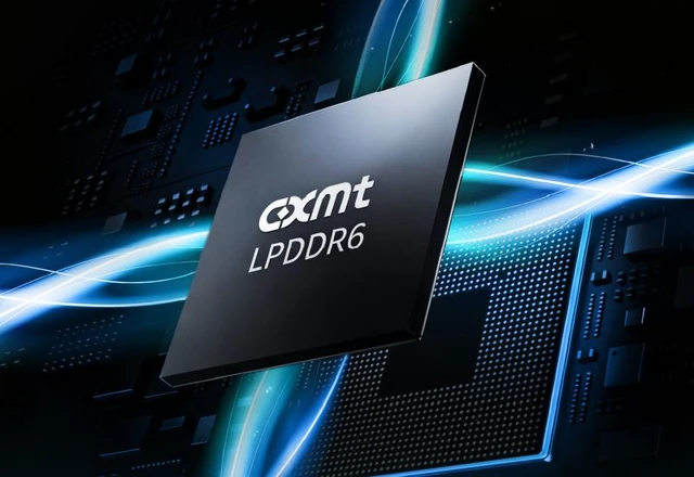
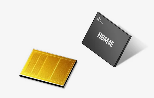
This technological foundation serves as the bedrock for next-generation products. The 1c node will underpin future LPDDR6 and DDR5 standards, as well as high-performance HBM4E memory. Simultaneously, the more mature 1b process continues to supply the market with essential solutions such as HBM3E and HBM4, which are already critical for the operation of modern GPUs and AI accelerators.
The competitive landscape in this segment is intensely fraught. Currently, Samsung and Micron maintain a slight lead in 1c adoption rates (16% and 19% respectively, compared to SK hynix's 13%). However, the South Korean manufacturer's scaling trajectory suggests a clear intent to seize the initiative by the fourth quarter of this year.
In the long term, the industry is colliding with a fundamental physical ceiling. The traditional 6F² planar transistor architecture has nearly exhausted its scaling potential. Further progress will require a radical reimagining of cell geometry: a shift toward 4F² vertical-gate transistors and full three-dimensional (3D) DRAM stacking. While these innovations will define the future, the 1c node will remain SK hynix's primary workhorse for years to come, providing the necessary equilibrium between density, power efficiency, and manufacturing cost.
 Power and Poise: The Xiaomi Pad 9 Pro Max