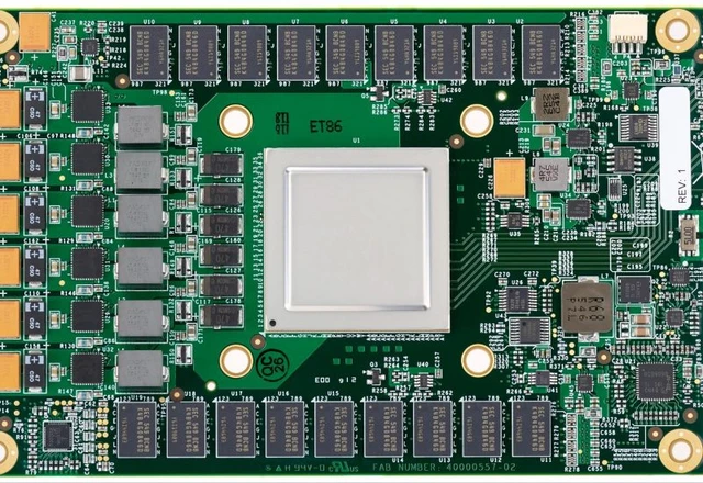
Modern microelectronics has reached a physical and economic impasse in traditional scaling, where every single nanometer of progress now demands an exponential surge in investment. Faced with a shortage of cutting-edge EUV lithography systems, the industry is pivoting its strategy to increase transistor density—shifting the trajectory of development from the horizontal plane toward verticality. Hybrid bonding technology has emerged as the critical bridge, enabling the unification of computing power not through cumbersome interfaces, but via the direct molecular fusion of dies. This marks a fundamental paradigm shift: the battle is no longer about shrinking the individual element, but about maximizing signal velocity and the efficiency of three-dimensional integration.
A fundamental paradigm shift is unfolding in the global pursuit of semiconductor performance. While industry giants strive to push lithography to its absolute physical limits, ambitious players—including startups like Yuanji Microelectronics—are betting on a radically different approach. Their objective is to achieve transistor densities equivalent to a "5-nanometer" process (approximately 130 million units per square millimeter) while completely bypassing the need for Extreme Ultraviolet (EUV) photolithography.
The catalyst for this breakthrough lies in the synergy between two pivotal technologies: the adoption of two-dimensional (2D) semiconductors and the implementation of hybrid bonding. In 2D transistors, the gates consist of structures only a single atom or molecule thick, forcing electrons to move strictly within a defined plane. This material property makes them ideal candidates for vertical stacking; traditional three-dimensional structures, such as FinFET or GAAFET, are too fragile and suffer from poor heat dissipation when attempted as part of a multi-layered "stack."
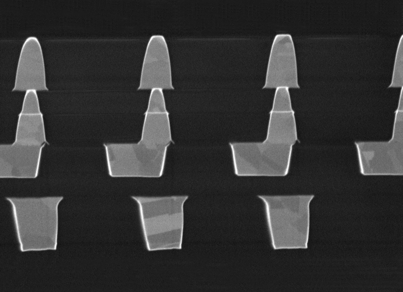
At its core, hybrid bonding eliminates the need for intermediary interconnects. In conventional chiplet designs, crystals are joined via microbumps—tiny solder droplets that, despite their size, introduce significant latency and limit interconnect density. Hybrid bonding, conversely, enables the direct mating of conductive buses that penetrate the chips vertically. While the most advanced microbumps provide a density of up to 1,600 contacts per mm², hybrid bonding has already demonstrated staggering results in Imec laboratories, reaching 7 million connections per square millimeter.
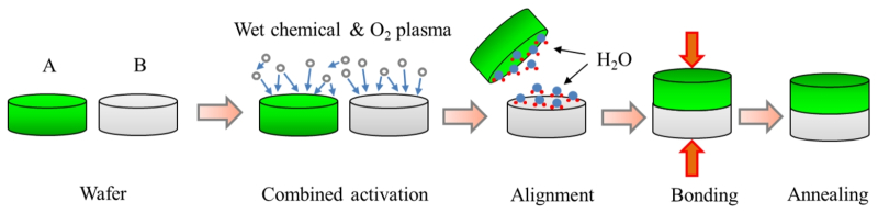
The fabrication process is akin to molecular surgery. First, the surfaces of two chiplets are polished to a mirror finish, achieving a roughness of just 0.1–0.2 nm. Copper pillars within the vias are not extended to the very edge, leaving a microscopic gap. Upon contact, the dielectrics of the two wafers adhere via weak Van der Waals forces. This is followed by an annealing stage—a controlled cycle of heating and cooling—during which the copper expands, fills the gaps, and forms a monolithic electrical connection.
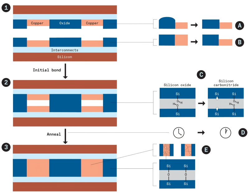
Yet, the road to commercial scalability is riddled with formidable engineering hurdles. A primary challenge is ensuring absolute surface planarity; the slightest deviation can result in contact failure or damage to the insulating layer. Furthermore, the high annealing temperatures (350–400 °C) can adversely affect silicon structures. Another critical concern involves grain boundaries within the copper channels, which create defects that impede current flow and heat dissipation, while also serving as potential points of mechanical fracture.
The industry currently distinguishes between two primary methodologies: wafer-to-wafer (W2W) and chip-to-wafer (C2W). Wafer-to-wafer bonding is technically more straightforward and allows for the smallest interconnect pitches (down to 400 nm), as lithography equipment is natively designed for the ultra-precise positioning of large substrates. However, from a practical standpoint, C2W is more valuable; it enables the integration of heterogeneous chiplets—for instance, placing SRAM memory blocks directly atop processor cores to optimize both spatial footprint and production costs.
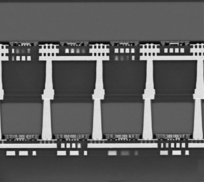
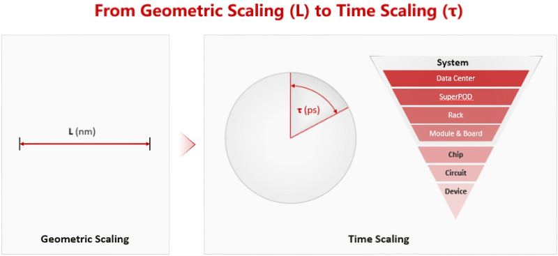
This pivot toward verticality has prompted Huawei to articulate the "Tau Law" ($\tau$). While Moore's Law focused on the spatial density of transistors, the Tau Law shifts the emphasis to the temporal component—the reduction of signal propagation delay within the circuit. For artificial intelligence workloads, minimizing latency in data transfer between memory and the compute core is far more critical than simply increasing clock speeds.
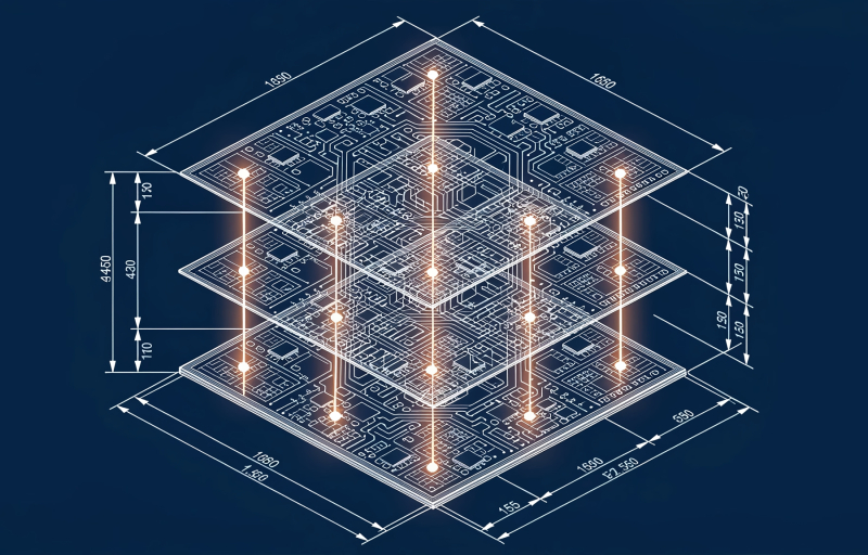
This conceptual framework finds its practical application in "LogicFolding." Rather than spreading logic blocks across a single plane—which creates long, slow data buses—LogicFolding involves "folding" the logic into multiple active layers. In the Kirin 2026 processor, this architecture enabled a 53% increase in transistor density (reaching 238 million units per mm²) and a 41% boost in energy efficiency, despite utilizing a less advanced lithographic process.
Vertical integration addresses several fundamental bottlenecks simultaneously: it radically shortens the signal path, reduces mutual electromagnetic interference between adjacent circuits, and mitigates clock skew—the synchronization lag that frequently limits the maximum frequency of modern processors.
Consequently, hybrid bonding is evolving from a mere assembly technique into a cornerstone of architectural design for future computing systems. The transition from flat design to multi-layered intelligent structures allows engineers to bypass the constraints of lithography, paving the way for ultra-high-performance systems where physical proximity defines computational efficiency.
 The Price of Acceleration: CXMT’s Rapid Push into Memory