The quest for truly ergonomic AR and VR wearables has long been stifled by the inherent physical constraints of traditional optics. Cumbersome lens arrays render headsets heavy and unwieldy, imposing a palpable physical barrier between the user and the digital realm. A breakthrough in metalens technology by South Korean researchers promises to disrupt this paradigm, replacing bulky glass elements with nearly weightless nanostructures. By overcoming the hurdles of chromatic aberration and manufacturing scalability, this innovation paves the way for an era of truly seamless, unobtrusive wearable displays.
Modern AR/VR optics are still tethered to principles that have remained largely unchanged for centuries: relying on the curvature of lens surfaces to focus light. This architectural approach inevitably leads to increased weight and bulk, transforming sleek glasses into cumbersome headsets. The alternative lies in metalenses—ultrathin optical elements that operate on entirely different physical principles. Rather than altering the geometry of the glass itself, they utilize a flat metasurface composed of millions of nanostructures, each smaller than the wavelength of light.
These nanostructures—essentially microscopic pillars—enable precise control over the phase, amplitude, and direction of photon propagation. In effect, a metalens mimics the refractive properties typically achieved through the thickness and curvature of glass, but does so within a single, razor-thin layer of material. This collapses a bulky lens stack into a lightweight plate that adds virtually no weight to the device.
Yet, the transition to flat optics hit a fundamental wall: chromatic aberration. Because different wavelengths of light—red, green, and blue—focused at different distances, the result was color fringing and a loss of image sharpness. The traditional remedy involved individually tuning the width of the nanopillars for each color, but this failed to resolve the issue of a unified focal point.
The breakthrough came with the introduction of height variability. By adding a third dimension to the nanopillar architecture, engineers were able to synchronize the focus for all primary colors, delivering a crisp, full-color image. However, this advancement introduced a new challenge: manufacturing elements with varying heights proved significantly more complex than standard processes.
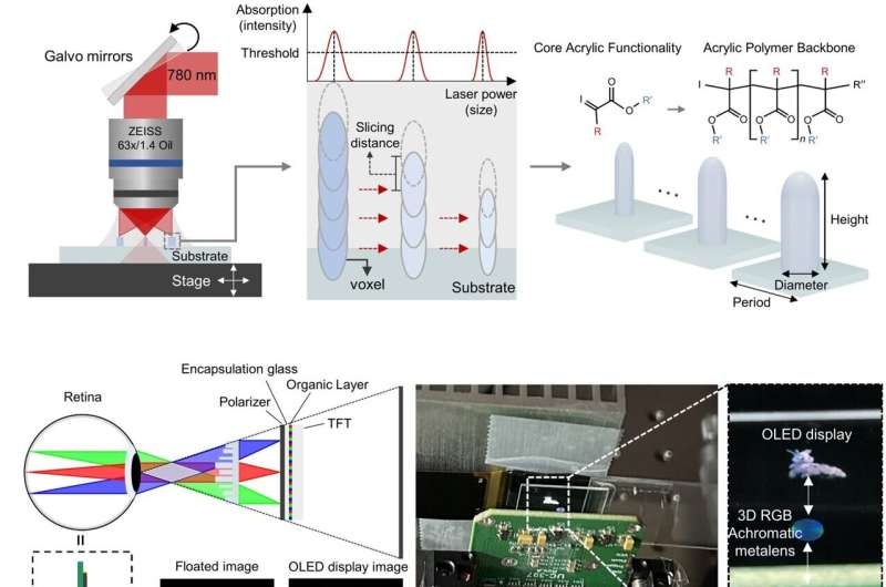
The primary bottleneck for commercialization was the inability to mass-produce these complex reliefs. Traditional nanoimprint lithography, which operates on a stamping principle, requires a uniform imprint height across the entire surface. To overcome this limitation, a hybrid methodology was developed, merging electron-beam lithography with nanoimprinting. This allows for the creation of high-precision stamps with complex reliefs, which can now be used for the serial production of metalenses.
This technological pivot resonates far beyond the realm of consumer VR headsets. The capacity to engineer ultralight, high-efficiency optical elements opens new frontiers for imaging systems, medical sensors, and compact cameras. In the long term, this signals a shift from cumbersome hardware to elegant frames that are virtually indistinguishable from ordinary eyewear, while maintaining the full functionality of modern digital interfaces.

 Pushing the Limits of the Google Pixel 11 Pro Fold