The transition from conventional electronics to photonic computing demands a fundamental overhaul of fabrication methodologies—a paradigm where extreme precision must coexist with industrial-scale throughput. For years, ion-beam lithography has been hampered by its inherently sequential nature, rendering the creation of nanostructures a painstakingly slow endeavor. A novel approach to component patterning is now breaking this bottleneck, slashing wafer processing times from several hours to a matter of seconds. This breakthrough paves the way for the mass production of intricate 3D photonic circuits that were previously confined to the controlled environments of research laboratories.
In modern microelectronics, there is a fundamental tension between throughput and resolution. While classical photolithography offers immense productivity, it is bound by the diffraction limit of light. Conversely, ion-beam lithography allows for far more stringent technological nodes, enabling the creation of structures of nearly any complexity; however, its Achilles' heel has always been speed. An ion beam operates like an ultra-fine pencil, "drawing" each element sequentially. Consequently, processing even a tiny area of 100 by 100 micrometers could take roughly seven minutes, rendering the method impractical for mass production.
To resolve this impasse, researchers from the Institute of Physics at the Chinese Academy of Sciences, in collaboration with colleagues from the University of Hong Kong, have proposed a novel concept: "ion-beam induced origami." This approach shifts the process from sequential drawing to parallel action. Rather than treating each element individually, the scientists employ a wide, parallel beam of argon ions that acts upon the entire silicon wafer simultaneously.
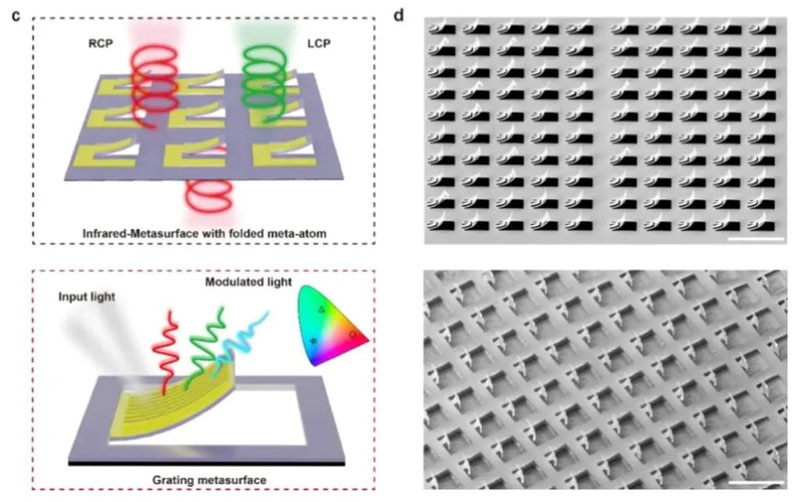
The fabrication process begins with the creation of flat templates on silicon nitride membranes using electron-beam lithography. These structures are coated with a thin layer of gold, forming a bilayer system where each layer is approximately 50 nm thick. When subjected to wide-beam argon ion irradiation, controlled defects and internal mechanical stresses emerge within the near-surface layer. These stresses force the pre-engineered flat elements to bend in synchrony, transforming them into precise three-dimensional architectures. The entire transformation of the array takes roughly 20 seconds—effectively accelerating this production stage by more than a hundredfold.
The method's efficacy is validated by its high degree of uniformity: over 97% of the nano-elements on a 4-inch wafer achieve the required geometry in a single pass. This is a critical metric for industrial adoption, as structural variability in photonics leads to phase shifts and signal degradation.
To demonstrate the technology's practical utility, two distinct devices were developed. The first is a 3D chiral metasurface designed for controlling the circular polarization of light; it demonstrated an impressive circular dichroism value of 0.8 at a wavelength of 3.41 μm, enabling the efficient separation of left- and right-handed polarizations. The second is a bendable plasmonic grating, whose resonance can be tuned by more than 150 nm within the visible spectrum simply by altering the structure's curvature.
Such capabilities position this technology as a promising foundation for a new generation of polarization sensors, high-precision spectral filters, and integrated photonic circuits—the building blocks of future optical communication networks. Although the acceleration applies to only one stage of production, eliminating this "bottleneck" significantly brings the commercial availability of complex photonic chips closer to reality. The next phase will involve a detailed analysis of structural durability and a comprehensive cost assessment for full-scale factory implementation.
 The Horizon of China's Technological Sovereignty in Lithography