The race toward sub-2nm process nodes is entering a phase of extreme resource strain and peak engineering ingenuity. At the heart of this battle are ASML's High-NA EUV scanners, which enable unprecedented precision in patterning circuitry. Yet, the staggering cost of the hardware and the complexities of integration have driven a wedge between the strategies of the industry's dominant players. The industry is now witnessing a clash between TSMC’s measured caution, Intel’s aggressive offensive, and the calculated pragmatism of South Korean memory manufacturers.
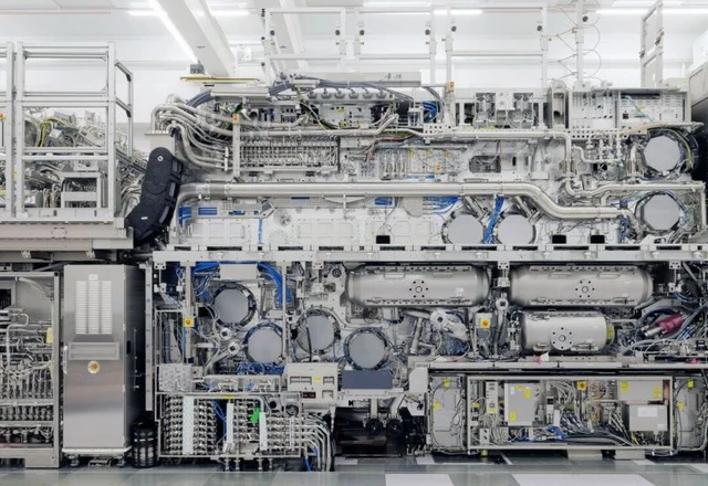
Modern microelectronics has arrived at a critical threshold where traditional lithography methods are reaching their breaking point. The solution lies in the transition to High Numerical Aperture (High-NA) systems, which enable a radical increase in printing resolution, allowing chip elements to shrink toward the physical limits of silicon. With a single scanner costing upwards of $400 million, upgrading production facilities has become one of the most expensive capital investments in the history of the technology sector.
Currently, ten such systems have been integrated into the production cycles and research laboratories of four key ASML clients. Intel has emerged as the vanguard of this transition, betting on an aggressive overhaul of its equipment fleet. The company is already leveraging High-NA capabilities for critical stages in the production of its Panther Lake processor family under the Intel 18A process, aiming to reclaim technological leadership through a radical reduction in transistor size.
Simultaneously, the TwinScan EXE:5200B systems are finding their niche in the memory sector. Samsung and SK hynix view High-NA not merely as a means of miniaturization, but as a strategic tool for optimization. In DRAM production, these scanners can cover up to five generations of lithographic norms, significantly simplifying tooling and shortening the overall production cycle. Amidst global shortages and surging demand for high-performance memory, such efficiency becomes a critical competitive advantage.
The equipment's technological maturity is validated by hard metrics: High-NA systems have already processed over 1.35 million silicon wafers. The current throughput of the TwinScan EXE:5200B stands at 135 wafers per hour, rendering it viable for mass production. However, this is only the beginning. By the end of the decade, ASML plans to introduce updated models capable of processing between 180 and 210 wafers per hour, which will significantly drive down the unit cost of each individual chip.
In contrast, TSMC, the world's preeminent foundry, is maintaining a markedly conservative stance. Despite acquiring several next-generation scanners, the company has limited their use to laboratory experimentation. For a giant of TSMC's scale, transitioning to High-NA in mass production entails colossal capital expenditures and the risk of restructuring the entire production chain. TSMC prefers to rigorously verify the economic viability and technical stability of the method before scaling it across its primary production lines.
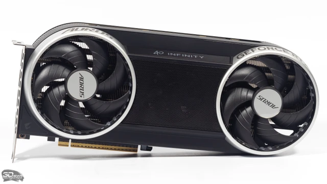 Aesthetics and Power: The AORUS GeForce RTX 5070 INFINITY