The modern AI industry is grappling with a critical deficit in computational capacity—a gap that cannot be bridged by mere shrinks in process nodes. Conventional chip-to-chip interconnects have become the primary bottleneck, stifling the scalability of large-scale neural networks. The path forward lies in the shift toward heterogeneous integration and the embedding of silicon photonics directly into the processor architecture. This strategic pivot promises a fifty-fold increase in system performance by the end of the decade.
The era of traditional semiconductor scaling is reaching its physical limits. With the demand for AI training and inference resources quintupling annually, the industry faces a stark ultimatum: pioneer fundamentally new system architectures or accept a stagnation in performance growth. In this climate, heterogeneous integration has emerged as the only viable path forward.
The core of this approach is the transition from monolithic dies toward complex, multi-layered structures. Central to this evolution are CoWoS (Chip-on-Wafer-on-Substrate) packaging and System-on-Integrated-Chip (SoIC) integration. The roadmap envisions a phased migration toward ultra-dense 3D structures: by 2026, the industry expects the deployment of N2P-on-N3P configurations, evolving by 2029 into the A14-on-A14 standard with an interconnect pitch of just 4.5 $\mu$m. This strategy allows for the fusion of disparate process nodes into a single computational unit, radically slashing physical distances between components and, consequently, signal latency.
Yet, even the most aggressive packaging cannot fully resolve the challenges of power consumption and thermal throttling associated with high-speed data transmission. This is where silicon photonics enters the fray—a technology that converts electrical signals into light directly within the chip.
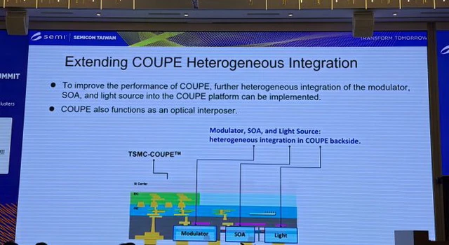
The linchpin of this transformation is the COUPE (Compact Universal Photonic Engine) platform. It enables the seamless integration of Electronic Integrated Circuits (EIC) with Photonic Integrated Circuits (PIC) via high-precision interconnects. The results are striking: transmission losses at 112 Gbps plummet from 1.38 dB (using traditional micro-bumps) to a negligible 0.06 dB. This is not merely an optimization; it is a paradigm shift that reduces latency to the 10–20 nanosecond range and significantly lowers the system's thermal footprint.
To sustain bandwidth growth, development is proceeding along two primary vectors. First, increasing per-channel transmission speeds from 200 Gbps to 400 Gbps while simultaneously expanding the channel count from 16 to 128. This pushes total throughput from 3.2 to over 12.8 Tbps. The second vector is the implementation of Wavelength Division Multiplexing (WDM), effectively creating a multi-lane "optical superhighway" within a single physical connection.
The shift toward Co-Packaged Optics (CPO) necessitates a complete overhaul of design and quality control processes. To mitigate the risk of costly failures during final assembly, optical testing is being implemented directly at the wafer level. Concurrently, specialized electro-photonic simulation platforms are being developed, integrated with Cadence and Synopsys tools, allowing engineers to predict signal behavior long before the chip ever hits the fab.
On a global scale, we are witnessing an architectural pivot in data center design. Optics are evolving from simple external server interfaces into the "neural backbone" of the entire computing complex. Projections suggest that by 2027, silicon photonics will command over 50% of the optical transceiver market.
Despite the technological readiness for mass production, the primary bottleneck remains the supply chain. While the reliability of silicon substrates has been proven in practice, the industry remains dependent on external components: precision lasers, specialized optical fibers, and high-precision connectors. These specific links currently dictate the actual pace at which photonic computing expands across the global IT infrastructure.
 The Korea-Japan Technological Alliance