The pursuit of extreme display miniaturization has long been stalled by a fundamental conflict between organic chemistry and semiconductor fabrication processes. Modern requirements for augmented reality devices and biomedical sensors demand pixel densities that are simply unattainable via traditional deposition methods. Researchers at ETH Zurich have bridged this gap by marrying the versatility of OLED materials with the precision of photolithography. This breakthrough enables the creation of emissive structures on the scale of single-celled organisms, ushering in a new era of micro-optics.
The primary obstacle to engineering ultra-miniature OLED displays has long been a fundamental chemical incompatibility. Conventional semiconductor fabrication relies on photolithography—a process demanding aggressive solvents and reagents to etch precise patterns. However, the organic light-emitting molecules central to OLED technology are hypersensitive to such environments, degrading instantly when subjected to the "etching" required for microscopic patterning. The industry was thus caught in a dichotomy: opt for the stability of silicon at the cost of flexibility, or embrace organics while sacrificing resolution and positional precision.
Swiss researchers have resolved this paradox by synthesizing a novel class of polymers that merge the functions of a light emitter and a photoresist. The material now dictates its own geometry under ultraviolet exposure. This transforms display fabrication into a form of "optical printing," where UV radiation carves microscopic, luminous elements of precise geometry directly onto the chip's surface.
The technological cornerstone of this breakthrough is a specialized "core-shell" molecular architecture. At the center of each molecule lies an active organic component responsible for generating a specific light spectrum, encased in branched, star-shaped chains that serve as sites for chemical reactions. Upon UV irradiation, these external chains cross-link, forming a dense polymer network. This shell acts as a protective barrier, insulating the luminescent core from aggressive chemicals during processing and preserving its functional integrity.
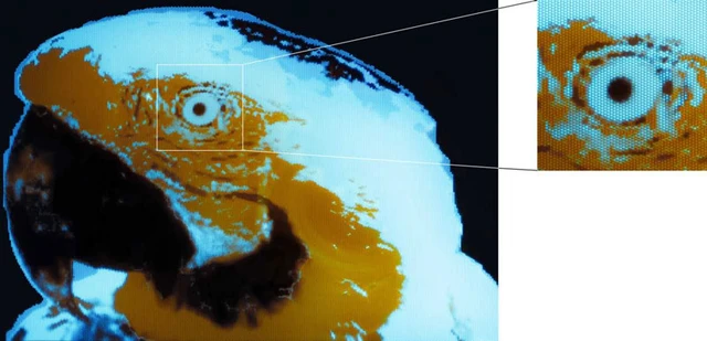
Practical demonstrations of this method have yielded objects on a scale comparable to simple microorganisms. Among the most striking results is a multicolored fluorescent image of a macaw. Measuring just 300 by 430 micrometers, the image boasts a fill density of 250 by 350 pixels—currently the highest resolution ever achieved for multicolored structures produced via photolithography.
However, the technology's true potential is revealed in the transition from static imagery to active devices. The team has developed a functional prototype of the ETH Zurich logo, measuring 1 by 2.4 millimeters, where each LED element is electrically controlled. Unlike the initial proof-of-concept, which required external light for activation, this device constitutes a fully realized micro-display.
The implications of this development extend far beyond consumer electronics. While it paves the way for ultra-high-density displays in AR glasses, the technology also unlocks profound possibilities for biomedical integration. The ability to engineer pinpoint light sources capable of interacting with individual cells or neurons could lead to a new generation of microscopy tools and neuromodulation systems, where light becomes a precision instrument for controlling biological processes.
 The Kinetic Aesthetics of the Titanium Sakura