Modern microelectronics has reached a critical juncture where traditional transistor scaling is hitting a wall of diminishing returns. The transition from planar structures to 3D FinFET and GAAFET was merely an evolutionary stepping stone in the relentless pursuit of packing density and energy efficiency. Today, CFET technology takes center stage, proposing a radical reimagining of logic element topology itself. This paradigm shift promises to serve as the foundation for next-generation computing architectures capable of sustaining the escalating demands of increasingly complex AI models.
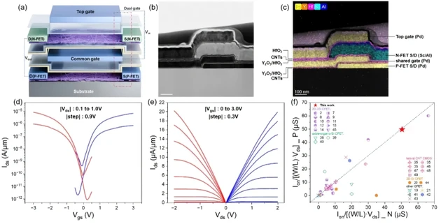
The semiconductor industry has entered a period of profound transformation. Among the most significant recent milestones is the breakthrough by a research team at Peking University, which successfully developed fully functional logic circuits based on Complementary Field Effect Transistors (CFETs) utilizing carbon nanotube channels. The results are striking: an amplifier built on this architecture demonstrated a peak gain of 164 at 1.0 V—a record for such circuits. Furthermore, the developers implemented basic logic elements (NOR, OR, NAND, AND), a 4T-SRAM static memory cell, and even a monolithic sensing-computing circuit capable of detecting faint infrared radiation streams.
This success validates the viability of the CFET concept and paves the way for ultra-compact, AI-centric computing units where silicon photonics and nanotubes operate in seamless tandem.
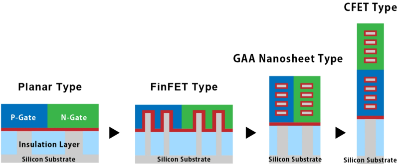
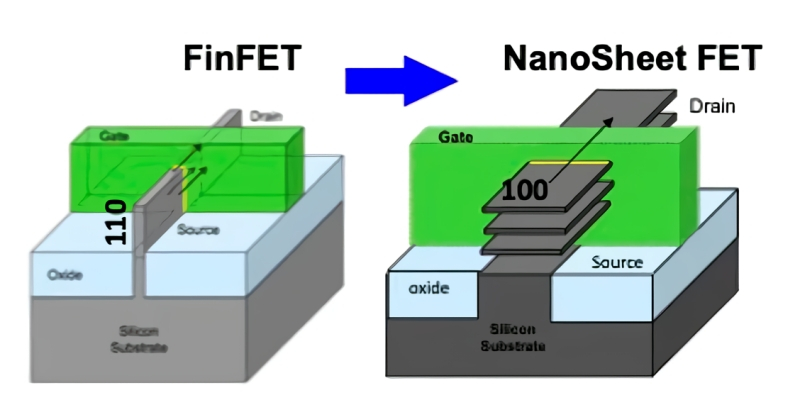
To appreciate the significance of CFETs, one must trace the evolution of the fundamental "building block" of electronics. In a classic planar MOSFET, the source, drain, and channel all reside on a single plane of the silicon wafer. As process nodes evolved, the industry transitioned to FinFETs, where the channel takes the form of a "fin" protruding from the substrate. While this provided superior control over leakage current, it introduced challenges regarding crystallographic orientation: utilizing planes with a Miller index of 110 reduced electron mobility and increased defect density compared to the ideal 100 orientation.
The next leap was the Gate-All-Around FET (GAAFET), where the gate completely envelops nanosheet channels. This architecture allowed for a substantial increase in drive current without raising the operating voltage—a critical requirement, as modern dielectrics only a few nanometers thick cannot withstand high voltages without triggering dielectric breakdown or quantum tunneling.
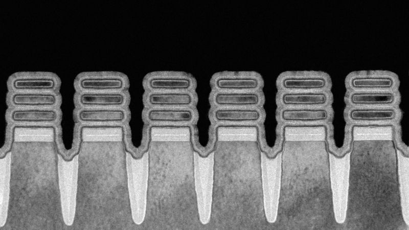
However, even GAAFETs struggle with the spatial separation of n-type (electron) and p-type (hole) conduction zones. In any planar or partially volumetric structure, these zones must be kept apart by a specific distance to prevent parasitic channels. Attempts to bring them closer using "forksheet" structures only partially mitigate the issue; as dimensions continue to shrink, the risk of insulator breakdown between the n- and p-regions only intensifies.
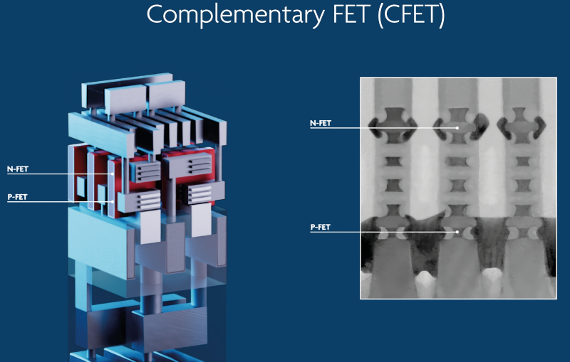
This is where the primary advantage of CFET emerges. In this concept, transistors are not placed side-by-side but are stacked vertically: the n-type device is positioned directly atop the p-type device. This completely eliminates the problem of lateral separation between conduction zones on the wafer, allowing components to be packed with the absolute minimum possible spacing.
Beyond density, CFETs offer a massive advantage in interconnect topology. In traditional circuits, a "tower" of metal buses and dielectrics (sometimes exceeding ten layers) is constructed above the semiconductor layer to connect dispersed transistors. The vertical structure of CFET allows connections to be organized directly within the gate planes, reducing the number of metallization levels to just one or two. This not only lowers the overall chip height but also radically simplifies heat dissipation, clearing the path for higher processor clock speeds.
Despite its theoretical elegance, integrating CFETs into mass production presents formidable technological hurdles. Two primary approaches have emerged: monolithic (mCFET) and sequential CFET.
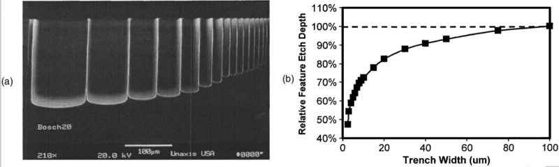
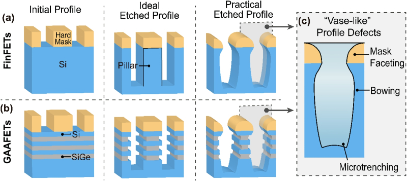
The monolithic method appears simpler as it relies on conventional layer deposition cycles. However, it suffers from the challenge of High Aspect Ratio (HAR). During the etching of deep, narrow trenches, an effect known as ARDE (Aspect Ratio Dependent Etching) occurs: the deeper the trench, the slower the reaction at the bottom. Consequently, the hole profile becomes "vase-shaped," leading to contact breaks or short circuits. Furthermore, the difference in ion and electron masses during plasma etching creates local electric fields that further distort the structure's geometry.
The second path—the sequential method—involves fabricating the two halves of the transistor (upper and lower) on separate wafers, followed by a precision layer transfer process to bond them. While this bypasses the ARDE problem, it introduces its own complexities: it is more costly, requires ultra-precise layer alignment, and limits the annealing temperature (to below 500°C) to avoid damaging previously formed structures.
Nevertheless, according to Imec roadmaps, the transition to CFET will become inevitable by 2030, roughly at the "A7" process node (marketed as 0.7nm). Once the potential of nanosheets is exhausted, the cost and complexity of vertical integration will become justifiable compared to the diminishing returns of refining GAAFETs.
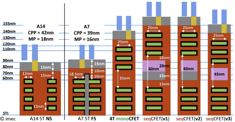
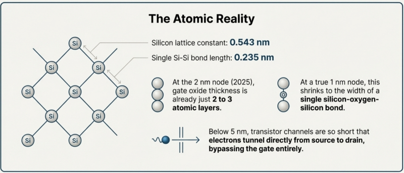
The global race for nanometers continues, and CFET appears to be the only realistic path to breaking the 1nm barrier. In an era where the demands of Large Language Models are growing exponentially and no mass-market alternative to silicon electronics yet exists, the industry will be forced to master vertical transistor construction. This is not merely an evolution of form—it is a transition to a new architecture of computing.
 Energy Autonomy: The Extreme Edition