The semiconductor industry has reached a physical impasse where standard EUV lithography can no longer sustain the requisite transistor density. The solution lies in the transition to High-NA systems, which leverage an increased numerical aperture to enable the fabrication of features below the 2-nanometer threshold. Despite the staggering capital expenditure required for such hardware, the relentless race for AI supremacy renders this technological leap an absolute necessity. The current pace of adoption reveals a profound strategic schism between the aggressive early adopters and the more cautious industry incumbents.
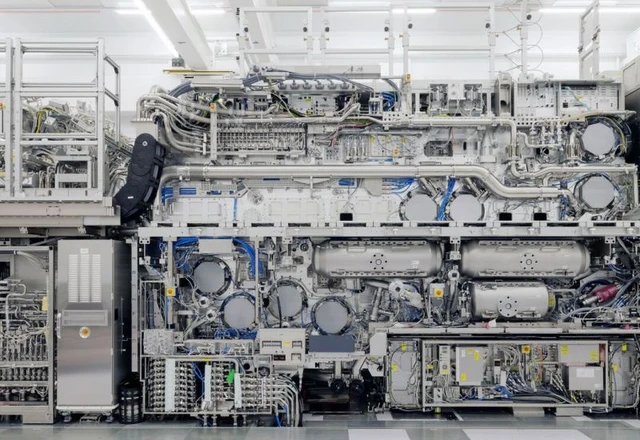
The current era of microelectronics is defined by a relentless battle for every nanometer, with Extreme Ultraviolet (EUV) scanners serving as the primary engine of progress. However, as the industry pushes toward sub-2nm process nodes, standard systems are reaching their limits. Enter High-NA (High Numerical Aperture) equipment—a paradigm shift in lithographic resolution that enables the printing of denser, more complex circuit patterns. This progress comes at a steep price: with single units costing up to $400 million, acquiring such a scanner is no longer just a procurement task, but a high-stakes strategic maneuver.
The market is currently in a phase of cautious adoption. According to ASML, ten of these systems have already been integrated into the production cycles and research labs of four major clients, with another three currently being shipped and installed. This equipment does more than just refresh a fleet of machinery; it determines who will be the first to achieve mass production of next-generation chips.
Intel is pursuing the most aggressive strategy. The company has effectively become the pioneer in deploying High-NA for high-volume manufacturing, utilizing these systems to realize its Intel 18A process. Specifically, the equipment is being used to develop the Panther Lake processor family, underscoring Intel's ambition to reclaim technological leadership through the rapid mastery of cutting-edge lithography.
Simultaneously, South Korean giants Samsung and SK hynix are betting on the memory sector. For them, the TwinScan EXE:5200B systems are the key to the evolution of DRAM. It is expected that High-NA will enable the introduction of at least five new generations of lithographic standards in memory production. This not only increases data storage density but also significantly streamlines tooling and shortens the overall production cycle—a critical advantage amid the current shortage and surging demand for high-performance memory.
From a technical standpoint, High-NA systems are already demonstrating impressive efficiency. To date, the equipment has processed over 1.35 million silicon wafers. The current throughput of the TwinScan EXE:5200B stands at 135 wafers per hour, making it viable for mass production. However, there is significant room for growth: ASML plans to increase this figure to 180–210 wafers per hour by the end of the decade through the release of more advanced hardware iterations.
Against this backdrop, TSMC’s position appears notably conservative. Despite being the world's largest foundry, the Taiwanese giant has so far limited itself to laboratory experiments with the new scanners. For TSMC, transitioning to High-NA in mass production entails colossal capital expenditures that may be economically unjustifiable at this stage. The company prefers to wait until the technology is fully matured, ensuring that its implementation is maximally efficient and carries minimal risk given the sheer scale of its operations.
 The Strategic Alliance of Nvidia and MediaTek