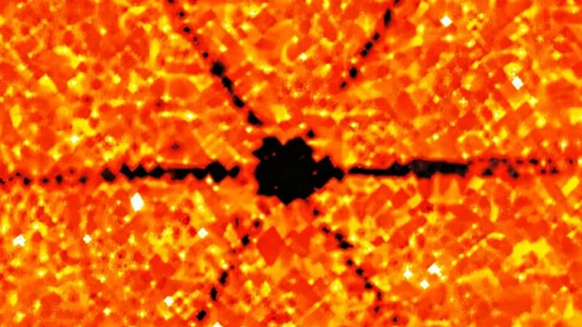
Modern microelectronics has collided with a fundamental physical ceiling in power consumption, rendering the quest for novel switching mechanisms a critical imperative. Amidst the relentless arms race for AI performance and mobile computing efficiency, traditional semiconductors are becoming prohibitively "hot" and increasingly inefficient. The solution may lie in a paradigm shift: moving away from the individual movement of electrons toward their collective behavior. To this end, US-based researchers have unveiled a prototype transistor that leverages quantum charge density waves to radically slash energy consumption.
Traditional electronics is predicated on the management of individual charge carriers. We are accustomed to viewing electrons as independent particles—entities that are either permitted to traverse a transistor channel or blocked by it. Quantum physics, however, offers a different paradigm: under specific conditions, electrons cease to behave like a disjointed crowd and begin to move in synchrony, manifesting their wave-like nature. This phenomenon is known as a Charge Density Wave (CDW).
To harness this effect, a team of researchers from the University of California, Los Angeles, turned to tantalum trisulfide ($\text{o-TaS}_3$). This quasi-one-dimensional material possesses a unique property: its electrons and crystal lattice form what is known as an electron-lattice condensate. In this state, the medium becomes an ideal conduit for the propagation of charge density waves, where the response to an external stimulus becomes collective rather than individual.
The experimental setup consisted of nanoscale field-effect transistor prototypes, featuring $\text{TaS}_3$ crystals only a few nanometers thick. Control was exerted via a gate that generated an electric field, while changes in charge density were monitored using high-precision radio-frequency (RF) measurements. The results were staggering: the system's response exceeded theoretical expectations—based on gate geometry and standard semiconductor calculations—by a factor of 10 to 100.
This effect implies that even an infinitesimally weak external stimulus can restructure the entire condensate. In a conventional transistor, current modulation depends on the number of electrons successfully "attracted" or "repelled" within the channel. With CDWs, we see a qualitative leap: the control field acts upon the collective state, triggering an avalanche-like response across the entire electronic system.
Beyond merely demonstrating amplification, the researchers conducted a profound analysis of the device's quantum properties. For the first time in such experiments, the contribution of individual electrons was clearly decoupled from the collective contribution of the charge density wave. This enabled the determination of the device's quantum capacitance and the construction of a detailed band diagram, effectively transforming a theoretical concept into an engineerable model.
From an industrial perspective, the most significant takeaway is that the conceptual architecture of these devices—comprising a channel, a gate, and field-based control—is virtually identical to existing silicon microelectronics structures. This suggests that integrating CDW materials may not require a wholesale overhaul of global chip fabrication lines.
While currently a prototype rather than a commercial product, the prospects are immense. Transitioning to current management via collective electron behavior enables the creation of memory elements and logic switches that consume orders of magnitude less energy while maintaining high output currents. This could be the technological breakthrough that allows the electronics of tomorrow to overcome the thermal barrier and reach a new echelon of energy efficiency.

 Semiconductors for 600°C Operation