The current race for AI supremacy has shifted its focus: the battleground is no longer defined by transistor density, but by the efficiency of data movement. Conventional copper interconnects have become a critical bottleneck, throttling both the throughput and power efficiency of next-generation supercomputing architectures. In this climate, government investment in silicon photonics has evolved beyond mere technological advancement—it is now a matter of national security. The strategic partnership between the U.S. government and GlobalFoundries is designed to forge a new data transmission infrastructure powered by light.
The semiconductor industry has reached a critical inflection point: the relentless pursuit of shrinking process nodes is colliding with the fundamental physical limits of materials. Recognizing the diminishing returns of competing in the sub-7nm race, GlobalFoundries has executed a timely strategic pivot. The company has shifted its focus from leading-edge logic chip production toward the advancement of silicon photonics—a technology that enables data transmission via photons rather than electrons directly within silicon structures.
This transition is driven by the escalating demands of the Big Data era and Generative AI. As traffic volumes grow exponentially, traditional copper interconnects are hitting a wall; they are prone to oxidation, generate significant thermal losses, and restrict bandwidth due to electromagnetic interference. Silicon photonics solves these bottlenecks, delivering near-instantaneous data transmission with minimal power overhead.
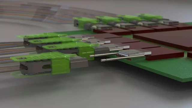
A new accord with the U.S. Department of Commerce, coupled with a $300 million allocation under the CHIPS Act, provides GlobalFoundries with the capital necessary for a deep modernization of its tech stack. The primary emphasis is on developing advanced packaging methodologies. Central to this effort are Near-Packaged Optics (NPO) and Co-Packaged Optics (CPO), which allow optical modules to be integrated as close as possible to the compute core, reducing signal travel distance to an absolute minimum. Combined with hybrid 3D bonding and novel materials, this enables the creation of ultra-dense computing systems.
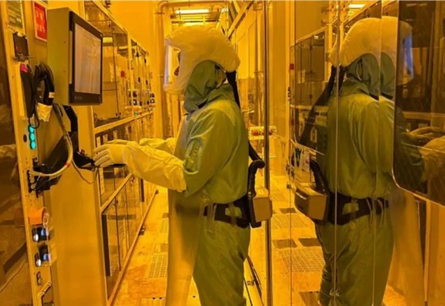
The tangible manifestation of these ambitions is the SCALE platform (Silicon Photonics Co-Packaged Advanced Light Engine). This system is capable of supporting packet transmission speeds of 400 Gbps—a critical benchmark for modern data centers. Investments will be directed not only toward R&D but also into expanding physical production capacity; manufacturing facilities in Malta, New York, and Burlington, Vermont, will receive the necessary upgrades to scale these technologies.
Industry titans—from Nvidia and AMD to Meta and Microsoft—are closely monitoring this trajectory. For them, transitioning from copper to light represents an opportunity to exponentially increase the performance of AI training clusters without a prohibitive surge in cooling costs. The U.S. government's equity stake (a 1% acquisition) underscores the project's status as a strategic imperative for the entire technological supply chain, ensuring the independence and resilience of domestic data transmission infrastructure.
 Scaling Next-Generation Chip Production