Modern microelectronics has hit the wall of physical scaling, forcing an industry-wide pivot toward heterogeneous integration. In this new paradigm, interposers and complex substrates are no longer mere connectors; they have evolved into sophisticated integrated circuits in their own right. However, traditional fabrication methods remain costly and fragile, shackled by a rigid reliance on physical photomasks. LG’s latest innovation proposes a radical departure: dynamic laser patterning—a shift that promises to fundamentally optimize production costs while unlocking unprecedented design flexibility.
The era of relentless process node shrinkage is gradually giving way to the age of advanced packaging. As traditional transistor scaling becomes economically or physically prohibitive, the industry is pivoting toward integrating multiple dies within a single package. This shift necessitates the development of high-tech interposers—intermediate layers featuring micron-scale routing and dense arrays of through-silicon vias (TSVs). In essence, the substrate is no longer merely a foundation; it has evolved into a complex electronic device in its own right, inevitably driving up production costs.
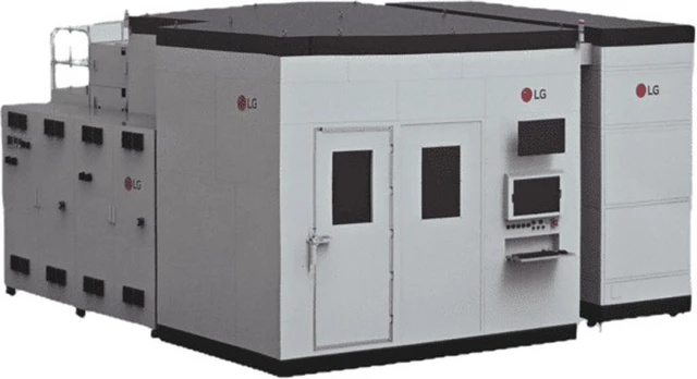
In response to these challenges, the LG Production Engineering Research Institute (LG PRI) has introduced a strategic solution: Laser Direct Imaging (LDI). This next-generation lithography system completely eliminates the need for physical photomasks. In today's market, where mask development costs and fabrication lead times can significantly bottleneck product launches, such an approach provides a decisive strategic advantage.
The technical implementation of the LDI system differs fundamentally from traditional steppers. Rather than projecting light through a physical template, the system utilizes a high-power laser diode generating ultraviolet radiation at a wavelength of 405 nm. This beam is directed onto a Digital Micromirror Device (DMD), consisting of millions of independently controlled mirrors. These mirrors form a dynamic image of the circuit in real-time and project it directly onto the photoresist layer. The result is conductors and gaps with widths ranging from 1.5 to 3 $\mu$m—a level of precision sufficient for the vast majority of substrate interconnect requirements.
One of the primary hurdles in large-panel production is mechanical instability; materials are prone to bending or warping. In traditional lithography, any surface deviation leads to pattern misalignment relative to the mask, resulting in defects. LG’s system mitigates this through Real-Time Active Compensation (RTAC). The equipment continuously measures substrate deformation and instantaneously adjusts the shape and position of the exposed image. This enables the efficient processing of panels up to 600 $\times$ 600 mm, whether they are standard printed circuit boards, silicon wafers, or cutting-edge glass substrates.
It is critical to understand where this technology fits within the broader semiconductor manufacturing hierarchy. LDI is not a competitor to ASML's EUV scanners, nor is it intended for printing nanometer-scale transistors. Its specialization lies in the "infrastructure" of the chip: forming contacts on the backside of silicon, creating micro-interconnects on interposers, and supporting advanced packaging methods such as FoCoS (Fan-Out Chip-on-Substrate) and CoPoS (Chip-on-Panel-on-Substrate).
The economic impact of implementing such systems becomes evident when dealing with High Bandwidth Memory (HBM) and modern processors. While a single unit costs approximately $2 million—a significant investment—the elimination of mask fabrication costs and the ability to pivot designs instantaneously make it indispensable for experimental runs and specialized orders. Ultimately, the transition to "digital" circuit drawing shortens development cycles and lowers the barrier to entry for creating complex multi-chip modules.
 The Phenomenon of Chinese 96GB AI Accelerators