The semiconductor industry is undergoing a fundamental paradigm shift: the relentless race for smaller nanometer nodes is giving way to the era of advanced chip packaging. Amidst critical capacity constraints at TSMC, the market is increasingly desperate for alternative solutions to develop sophisticated multi-chip modules. Intel views this as a strategic window of opportunity, offering a technology stack designed to satisfy the voracious demands of the AI industry's leading players. This specific segment may well be the fastest route toward ensuring the financial sustainability of the company's foundry business.
As Moore's Law decelerates and the costs associated with monolithic die development scale exponentially, the industry is pivoting toward a chiplet-centric architecture. In this new landscape, efficiency is no longer defined solely by transistor density, but by how effectively discrete compute blocks are integrated into a unified system. This is where Intel is placing its bet on advanced packaging services—a venture capable of generating profitability far more rapidly than traditional silicon wafer fabrication.
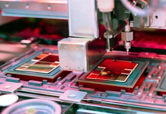
At the heart of this strategy lies Embedded Multi-die Interconnect Bridge (EMIB) technology. While the market has long been tethered to TSMC's CoWoS solution, EMIB offers a comparable—and in some respects, superior—alternative. Its primary advantage lies in the ability to bypass the physical constraints of the reticle limit—the maximum area printable in a single lithography cycle. Through EMIB, Intel can integrate components with a combined area nine times larger than the standard monolithic limit, reaching an impressive 120 × 120 mm.
However, for the demands of modern artificial intelligence, sheer scale is insufficient; the priority has shifted toward radical latency reduction and power optimization. Intel addresses this challenge with EMIB-T. This iteration introduces additional interlayer interconnects that optimize power delivery and shorten signal paths between compute cores and memory. For developers of complex accelerators, such as TPUs, this translates into significant gains in both performance and energy efficiency.
This technological arsenal has already caught the eye of strategic industry leaders. Reports suggest that Broadcom and Google, currently collaborating on specialized AI silicon, are deeply interested in Intel's capabilities. Meta and MediaTek are also on the list, seeking to diversify their supply chains and mitigate reliance on the overextended capacity of the Taiwanese giant, TSMC.
For Intel, this pivot represents a fundamental paradigm shift. Once focused exclusively on its own silicon, the company is evolving into a comprehensive service provider for the entire industry. By the second half of next year, packaging services are expected to become a significant revenue stream, transforming a technological edge into a tangible market asset.
 The Horizon of China's Technological Sovereignty in Lithography