The relentless pursuit of electronic miniaturization inevitably brings engineers face-to-face with the fundamental constraints of physical chemistry. While inkjet printing offers the promise of cost-efficiency and scalability, the notorious "coffee ring effect" consistently undermines the precision of the deposited layers. Conventional strategies to mitigate this phenomenon often come at a cost, compromising the final performance characteristics of the resulting conductors and semiconductors. Now, researchers at Tokyo Metropolitan University have proposed an elegant solution, drawing inspiration from the fluid dynamics of common carbonated beverages.
At the heart of modern additive electronics lies the precision deposition of functional inks infused with nanoparticles. However, as a droplet dries, it triggers a classic physical phenomenon known as the "coffee ring effect." Due to more intense evaporation at the edges of the droplet, a capillary flow is generated, transporting dissolved particles from the center toward the periphery. The result is a ring-like accumulation of material with a hollow center—a critical failure in microcircuitry, where thickness uniformity directly dictates the electrical resistance and optical properties of the component.
For years, the industry attempted to resolve this issue through chemical means by incorporating surfactants into the ink composition. These compounds alter the liquid's surface tension in an effort to balance the particle flow. However, this approach possesses a fundamental flaw: the chemical additives remain embedded within the printed layer, contaminating the structure and distorting the physical characteristics of the finished device. Ultimately, the struggle to perfect the layer's geometry comes at the cost of its functional integrity.
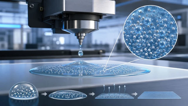
Japanese researchers have proposed a radical alternative, replacing chemical modification with physical intervention. They introduced sub-micron gas nanobubbles into the suspension. This concept, borrowed from the principles of carbonating beverages, allows for the alteration of the droplet's spreading and evaporation dynamics without changing the chemical composition of the material itself.
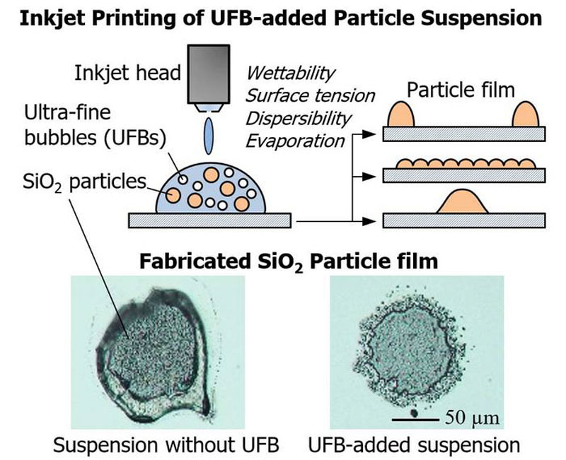
The mechanism behind these nanobubbles is the suppression of capillary transport. The gas bubbles within the droplet act as a physical barrier and redirect internal fluid flows, preventing nanoparticles from migrating to the edges. Crucially, this process is controllable: by varying the concentration of bubbles, researchers can essentially "orchestrate" the distribution of the matter. Moderate carbonation achieves ideal film uniformity, while a high concentration of bubbles causes the particles to concentrate in the center of the spot.
This level of control unlocks vast potential for the production of printed electronics, high-precision sensors, and microelectromechanical systems (MEMS). In these fields, even a marginal variance in layer thickness can lead to critical device failure or a complete loss of functionality. The ability to manage surface morphology through a purely physical method, bypassing the need for complex solvents, significantly streamlines the technological cycle.
At this stage, the technology has been successfully validated using model inks containing silicon oxide ($\text{SiO}_2$) nanoparticles. The next phase will involve testing the method on industrial-grade compositions: conductive silver or copper inks, as well as semiconductor materials. The primary engineering hurdle remains ensuring the long-term stability of the nanobubbles and their consistent behavior within multi-nozzle print heads, where fluid pressure and delivery speeds are exceptionally high.
 Navigating via Earth's Gravitational Anomalies