The global semiconductor market has evolved into a theater of intense geopolitical rivalry, where access to cutting-edge technology has become the primary lever of strategic pressure. At the heart of this struggle lies lithography—the intricate process of etching microchip architectures onto silicon wafers—a domain dominated for decades by a small oligopoly of Western firms. Faced with mounting sanctions, China has pivoted from a procurement-based strategy toward the ambitious goal of developing its own indigenous technological stack. The battleground has now shifted toward Deep Ultraviolet (DUV) lithography systems, which are poised to become the cornerstone of the PRC's digital sovereignty.
The chronicle of the modern technological standoff began with Huawei, which was the first to bear the brunt of American sanctions. Over the years, the company has evolved from a consumer electronics manufacturer into a sort of national orchestrator of import substitution. Today, the efforts of Huawei and its affiliated entities are concentrated on the most formidable challenge in microelectronics: the development of proprietary lithography equipment.
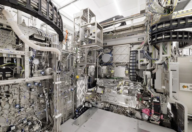
The focus is on Deep Ultraviolet (DUV) systems. While they sit below the cutting-edge Extreme Ultraviolet (EUV) scanners in the semiconductor hierarchy, DUV systems remain the industry workhorses for producing the vast majority of chips. Export restrictions on equipment from the Netherlands-based ASML have forced China to seek domestic alternatives, sparking the emergence of new market players.
A pivotal link in this chain is the Shanghai-based company Yuliangsheng. Despite official claims of independence, it maintains close ties with the startup SiCarrier, which analysts believe is effectively coordinated by Huawei's resources. This symbiosis has resulted in the development of a DUV-class lithography system, prototypes of which are already undergoing testing at SMIC—China's primary semiconductor foundry.
At this stage, the equipment is being used to create less complex components; however, SMIC engineers are attempting to push the boundaries of the possible. Specifically, they are trying to adapt a system designed for 28-nanometer processes to produce 7-nanometer chips. This is achieved through multi-patterning—a method where a single circuit layer is created using multiple photomasks. While labor-intensive and costly, this approach allows engineers to bypass the physical limitations of the hardware.
Yet, building a fully functional DUV scanner is not merely a matter of mechanical assembly; it is a battle against fundamental physical constraints. The primary bottlenecks remain high-precision optics and laser light sources. In this arena, Huawei has assumed the role of lead project manager, coordinating efforts across the entire industry.
The optical component is the most opaque sector of lithography. For years, the German firm Zeiss has held a virtual monopoly, supplying systems exclusively to ASML. To break this dependency, Huawei-backed investment funds, such as Habo and Shenzhen Yuanzhi Xinghuo, are financing Fujian Zhiqi Photonics. This entity is tasked with developing ultra-precision optical components capable of replacing Zeiss solutions. Notably, the roots of this initiative trace back to Castech—a company supported by the Chinese Academy of Sciences with experience working with both Western and domestic partners.
Equally critical is the issue of light sources. The global market is dominated by Japan's Gigaphoton and Europe's Cymer. The primary challenge for Chinese engineers lies in ensuring laser beam stability at extremely high power levels. In this direction, the strategic bet has been placed on Beijing's RSLaser Opto-Electronics, which already has a track record of supplying systems for previous-generation SMEE equipment.
Despite ambitious plans and the release of the first production samples, the reality remains stark. Mass production in China still relies on ASML equipment stockpiled before the imposition of stringent sanctions. Memory specialists, such as CXMT and YMTC, have built strategic reserves of components intended to last several years.
Western experts and analysts from Bernstein suggest that Chinese equivalents lag behind global leaders by at least 15 years. Nevertheless, sanction pressure has served as the catalyst, forcing China to invest colossal resources into fields that might have remained secondary in an open market. China is not merely building a lithography ecosystem as a replacement for imports, but as an attempt to completely rewrite the rules of the game in the semiconductor industry.
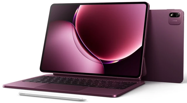 Power and Poise: The Xiaomi Pad 9 Pro Max