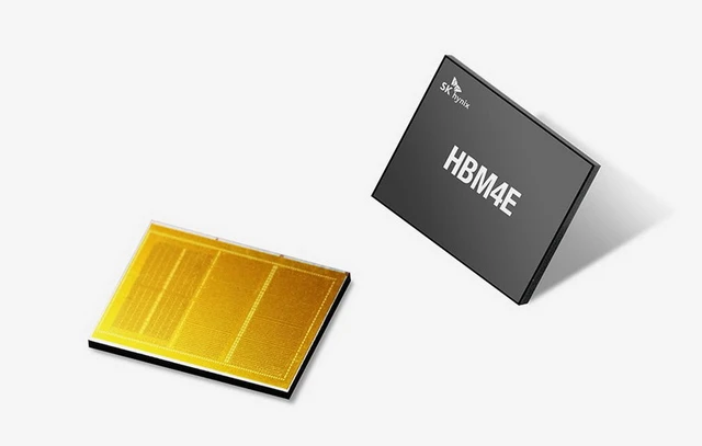
The meteoric rise of artificial intelligence has presented the hardware industry with a pivotal challenge: dismantling the "memory bottleneck." Conventional architectural paradigms can no longer deliver the requisite throughput without compromising energy efficiency. In response, SK hynix is spearheading a shift toward a radical paradigm—vertically stacking DRAM directly atop the logic die. This move signals a departure from incremental optimization in favor of a fundamental reimagining of the synergy between processing power and memory.
Modern neural networks, particularly Large Language Models (LLMs), are placing unprecedented demands on data exchange speeds between the computational core and system memory. As conventional packaging methods reach their physical limits, SK hynix is moving into an active development phase for its 3D-Stacked DRAM-on-Logic technology. The essence of this approach lies in creating a vertical "sandwich," where the dynamic memory layer is positioned directly atop the System-on-Chip (SoC) logic die.
The technological chasm between this method and the conventional Package-on-Package (PoP) configuration is vast. In traditional PoP schemes, memory chips and processors are connected via relatively long electrical paths, which inevitably leads to increased latency and higher power consumption for every bit of data transferred. Vertical integration allows for a radical reduction in interconnect length and a significant increase in I/O density per unit area. The result is a sharp decline in latency and a boost in overall system energy efficiency—factors that are critical for mobile devices and autonomous AI accelerators.
The strategic importance of this project is underscored by SK hynix's establishment of a specialized engineering task force within its San Jose division in the United States. This work is being conducted in close partnership with a major US-based client whose interests align with the creation of cutting-edge mobile platforms. It is evident that the primary beneficiaries of such technology will be market leaders in mobile processors, such as Apple and Qualcomm, as this segment faces the most stringent requirements for packaging density and power efficiency.
This initiative is not a random experiment but follows a strict corporate roadmap presented at the TSMC symposium. SK hynix leadership openly acknowledges that the era of linear memory scaling has come to an end. Further advancement in AI hardware requires qualitative leaps in memory architecture. As part of its collaboration with TSMC, the company plans to implement advanced logic processes into HBM4 base dies and extend the 3D-stacking concept to high-bandwidth flash (HBF).
Simultaneously, a competitive struggle is unfolding at the level of fundamental research. Samsung, in collaboration with imec and Lam Research, is exploring the possibilities of creating monolithic 3D DRAM using semiconductor oxide channels. Unlike SK hynix's pragmatic approach, which is oriented toward a market-ready product, Samsung's developments remain largely in the stage of theoretical modeling. Nevertheless, this highlights a global industry trend: the transition from flat topology to a fully three-dimensional space is becoming the only viable path to overcoming the "memory wall" in the age of artificial intelligence.
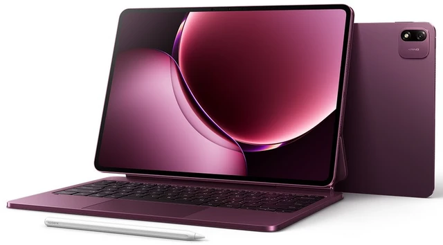 Power and Poise: The Xiaomi Pad 9 Pro Max