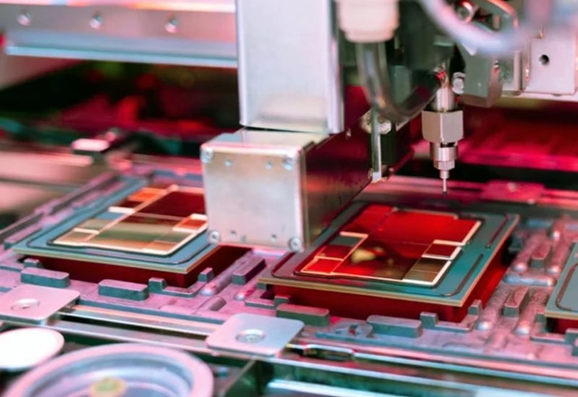
The pursuit of extreme transistor miniaturization is no longer merely a game of numbers; it has evolved into a high-stakes race for industrial scalability and deployment. Taiwan's semiconductor titan, TSMC, is demonstrating remarkable momentum in the development of its A14 process node, which—at its current level of maturity—is significantly outpacing its predecessor, N2. This trajectory underscores a profound mastery of next-generation lithography techniques and advanced die architecture management. The high-performance computing (HPC) and artificial intelligence sectors are now poised in anticipation of this transition—a shift that is set to define the landscape of electronics for the remainder of the decade.
The semiconductor industry is currently navigating a pivotal transition from traditional FinFET transistors to the more advanced Gate-All-Around (GAA) architecture. TSMC is demonstrating exceptional efficiency in this shift: the development of its A14 (1.4nm) process is advancing significantly faster than the N2 (2nm) node did at a comparable stage.
Recent internal tests of prototype components reveal that A14 performance has already reached 90% of its target benchmarks. Even more critical is the yield rate for 256Mb SRAM, which has also approached the 90% mark. For the industry, this serves as a clear signal of high structural uniformity and low wafer defect density—the primary predictors of a successful commercial rollout.
A comparative analysis of the development trajectories for these two processes highlights a qualitative leap. In April 2023, the N2 node delivered only 80% of its target performance with an alarmingly low yield of approximately 50%. A year later, these figures climbed to 90% and 80%, respectively. A14, however, has achieved similar or superior results in a much shorter timeframe. This acceleration is the direct result of accumulated expertise with GAA transistors, which debuted with N2. Essentially, TSMC has successfully ironed out the "teething problems" of the new technology, eliminating most bottlenecks during the design phase.
While mass production for A14 is slated for the second half of 2028, an early launch remains a distinct possibility. Demand from flagship smartphone manufacturers and AI system architects is so intense that clients are pushing to finalize their chip designs well ahead of schedule.
The technical advantages of A14 over N2 are compelling. The new process is expected to deliver a 10–15% performance boost while maintaining the same power envelope and transistor count. Alternatively, by keeping clock speeds and circuit complexity constant, power consumption could drop by 25–30%. Transistor density is also set to rise: by 20% for mixed-signal circuits and 23% for logic blocks.
One notable omission in A14 is the Super Power Rail—an innovative backside power delivery system designed to drastically reduce noise and reclaim valuable real estate on the chip's front side. Current roadmaps suggest this feature will debut with the subsequent A12 process, scheduled for the second half of 2029. Nevertheless, even without this capability, A14 represents a monumental leap forward, further cementing TSMC’s dominance in the cutting-edge semiconductor landscape.
 The Horizon of China's Technological Sovereignty in Lithography