For decades, the global memory market has been defined by a rigid oligopoly dominated by three technological titans. China's pursuit of total semiconductor sovereignty has now reached a critical inflection point. The commencement of mass production for fifth-generation DRAM by CXMT signals a strategic pivot—moving beyond cautious imitation toward genuine market competition. This move is poised to reshape global supply chains and fundamentally alter the economics of high-density memory manufacturing.
For years, the Dynamic Random Access Memory (DRAM) market has been dominated by the triumvirate of Samsung, SK hynix, and Micron. Any attempt to introduce a viable alternative has historically been thwarted by colossal technological barriers. However, CXMT's transition to a new production phase signals that China has found a way to scale its capacities, offering solutions that are beginning to converge with global standards in terms of performance and energy efficiency.
The cornerstone of this new platform is a radical increase in data density. Engineers have successfully reduced the spacing between critical memory cell elements to 11.95 nm. In the semiconductor industry, such precision is typically achieved either through prohibitively expensive Extreme Ultraviolet (EUV) lithography systems or via complex, multi-stage processes. CXMT has opted for Self-Aligned Quadruple Patterning (SAQP). This technique enables the creation of ultra-fine structures through repeated production cycles, effectively circumventing the limitations of conventional hardware and achieving high precision without relying on the latest Western scanners.
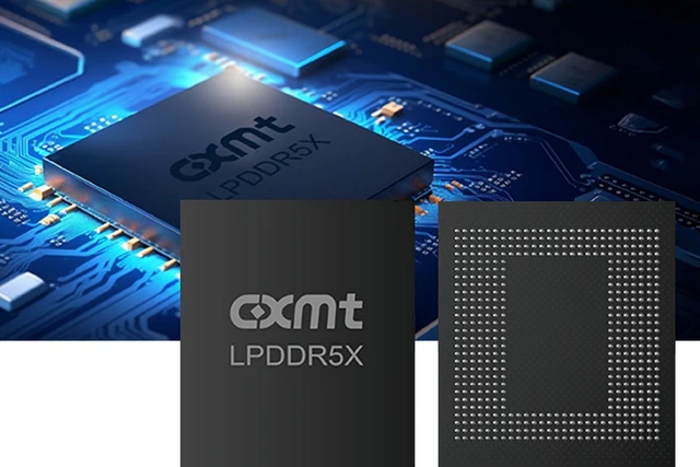
The culmination of this technological stack is the release of two new 24Gb LPDDR5X chips. This memory standard is pivotal for the modern mobile and portable electronics segment, where power consumption and data transfer speeds dictate overall system performance. These new chips deliver a 50% increase in storage capacity compared to the company's previous generation, making them highly attractive to smartphone and tablet manufacturers seeking hardware optimization.
Beyond raw performance, CXMT has focused heavily on manufacturing economic efficiency. A primary metric in the semiconductor business is the die yield—the number of functional chips obtained from a single silicon wafer. The new platform has increased the number of dies per wafer by 50% relative to the fourth generation. This translates to a significant reduction in unit cost, providing the company with the leverage to exert aggressive pricing pressure on its competitors.
CXMT's listing on Shanghai's STAR Market underscores the enterprise's strategic importance. This is not merely about the commercial success of a single vendor, but about establishing a resilient domestic supply of critical components. Amid global volatility and trade restrictions, the ability to produce cutting-edge memory internally has become a matter of national technological security.
Consequently, the shift to fifth-generation DRAM transforms CXMT from a local player into a serious contender in the reshaping of the global memory landscape. By combining innovative lithography methods with optimized die yields, the company is delivering a product that balances high data density with competitive pricing.
 Breaking the Lithography Barrier in China