The global quest for semiconductor sovereignty has escalated into a direct technological confrontation. Beijing is aggressively seeking to decouple from Western supply chains by developing indigenous Extreme Ultraviolet (EUV) lithography systems—the cornerstone of advanced chip fabrication. However, these ambitions are colliding with the stark reality of a significant engineering gap and the staggering complexity inherent in precision instrumentation. Thus far, China's push for import substitution in lithography has yielded only marginal success, overshadowed by the overwhelming market hegemony of the Netherlands-based ASML.
The semiconductor industry has found itself in the eye of a geopolitical maelstrom, where access to lithography equipment has become akin to controlling a strategic natural resource. Recent reports regarding the start of mass production for Deep Ultraviolet (DUV) systems within China have sent ripples through the financial markets. At the heart of this is immersion lithography—the critical technology required to manufacture the advanced semiconductors that serve as the foundation of modern electronics.
The first signs of this shift emerged through the activities of the Shanghai Aishengna Electronic Technology Group. Established just a year ago with the backing of Shanghai's municipal authorities, the entity has become a central hub for the nation's engineering capabilities. By integrating specialists from Shanghai Yuliangsheng and the more prominent SMEE (Shanghai Micro Electronics Equipment), China is attempting to forge a unified technological vanguard to break through Western embargoes.
The market responded to these developments with the volatility characteristic of the modern era. Shares of ASML and Infineon Technologies saw sharp declines, reflecting investor anxiety over the potential loss of the Chinese market. While analysts later dismissed this reaction as excessive, the fact that Chinese state media has begun hinting at the "eroding efficacy of the Western blockade" underscores Beijing's serious intentions.
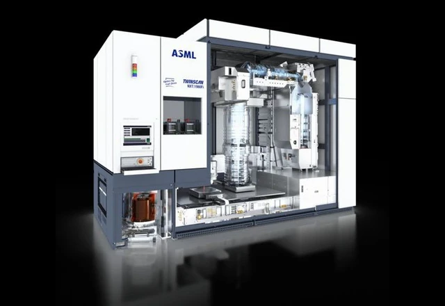
However, beneath the bold rhetoric lies a stark technical reality. Chinese DUV developments—specifically the SSX800 model—are comparable in specifications to the ASML Twinscan NXT:1950i. The problem is that the Dutch system was brought to market back in 2008. Consequently, China's current flagship is effectively four generations behind global industry standards.
The technological chasm is evident not only in the age of the systems but in their operational efficiency. While modern installations achieve exceptional yield rates—often reaching 90–95%—Chinese counterparts remain far from these benchmarks. Even with a throughput capacity of up to 150 wafers per hour, high defect rates render such systems commercially unviable for the full-scale mass production of high-end chips.
Furthermore, claims of "self-sufficiency" remain partial at best. Although the SSA800 system reportedly consists of 70% local components, critical subsystems—laser light sources, precision mirrors, complex optics, and control software—still rely on imports. This creates a paradox: in its quest to eliminate dependence on ASML, China remains beholden to supply chains that are still largely controlled by the West.
From a strategic standpoint, the internal division of labor within China appears logical: while Yuliangsheng and Aishengna strive to master the 28-nanometer process (with a target date of 2027), SMEE is focusing on the development of Extreme Ultraviolet (EUV) systems. However, the journey from prototype to industrial standard in lithography is measured in decades. For now, China's progress looks less like a genuine threat to ASML's technological dominance and more like a desperate strategy for survival under siege.
 Forecasting Exponential Growth in Nvidia Shipments