The global race for semiconductor sovereignty has long since evolved beyond a mere battle over nanometers, transforming into a critical imperative for national security and economic resilience. India is now vying for entry into this exclusive club by establishing its own silicon wafer fabrication infrastructure. Yet, the trajectory from ambitious blueprints to the first functional chip is invariably marked by a sobering encounter with the operational realities of semiconductor manufacturing. The case of Tata Electronics serves as a poignant example of how strategic objectives are recalibrated when confronted by sheer technological complexity and the pressures of tight timelines.
India’s strategic bid to establish a foothold in the microelectronics market began with an ambitious project in Gujarat, where Tata Electronics is constructing the nation’s first silicon wafer fabrication plant. While initial optimism pointed toward a rapid leap to 28nm process nodes, current dynamics suggest a more measured approach. The priority has now shifted toward mastering "mature" technologies—specifically the 90nm and 55nm processes.
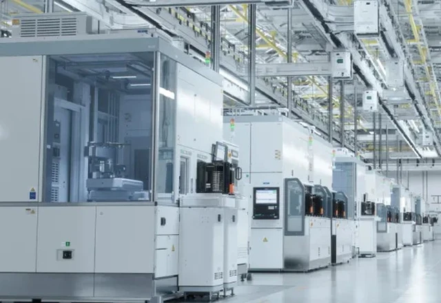
This pivot is not a sign of failure, but rather a reflection of industry pragmatism. Transitioning from simpler lithographic processes to more complex ones is standard practice for new entrants. To facilitate this, Tata Electronics has leveraged the support of Taiwan’s PSMC, which brings deep expertise in contract manufacturing. Partnering with Taiwanese specialists allows India to mitigate the risks associated with greenfield production by utilizing proven methodologies for cleanroom management and exposure precision.
Ultimately, the facility is designed to support a broad spectrum of process nodes, ranging from 110nm down to 28nm. Although 90nm technology is no longer cutting-edge, it remains critical for producing analog components, power controllers, and automotive electronics—sectors where stability and cost-efficiency outweigh transistor density. Simultaneously, the 28nm node remains highly relevant for a vast segment of consumer electronics and the Internet of Things (IoT), cementing its status as the project's primary strategic objective.
The financial architecture of this push is nuanced. While the Indian government recently approved $13.3 billion in subsidies to bolster new chip initiatives, Tata’s project—already underway—does not fall under this latest funding wave. Nevertheless, the venture relies on earlier state support programs, which may provide up to $5 billion toward a total estimated project budget of $10.7 billion.
Despite financial backing and technological partnerships, the project's timeline has undergone adjustments. Mass production in Gujarat is now expected to commence by mid-2028. This delay—approximately 18 months behind the original schedule—underscores the immense complexity of constructing modern fabs, where any misalignment in planning or equipment procurement leads to significant shifts in delivery dates.
In the long term, Tata Group intends to use the 28nm process as a foundation for advancing toward more sophisticated lithographic methods. This transforms the Gujarat plant from a mere production site into a technological proving ground, where India is learning to master the intricate orchestration of modern microelectronics.
 Nvidia N1X and the New Era of Arm PCs