The semiconductor industry has reached a critical inflection point, where traditional methods of scaling performance are colliding with insurmountable physical barriers. For years, the dominant paradigm focused on driving up transistor density and expanding die sizes; however, this trajectory is leading toward an inevitable technological dead end. Against the backdrop of the systemic rivalry between the U.S. and China, two fundamentally divergent philosophies of chip design are emerging. At the heart of this conflict lies a pivotal question: can architectural innovation bridge the gap created by a lack of access to cutting-edge fabrication equipment?
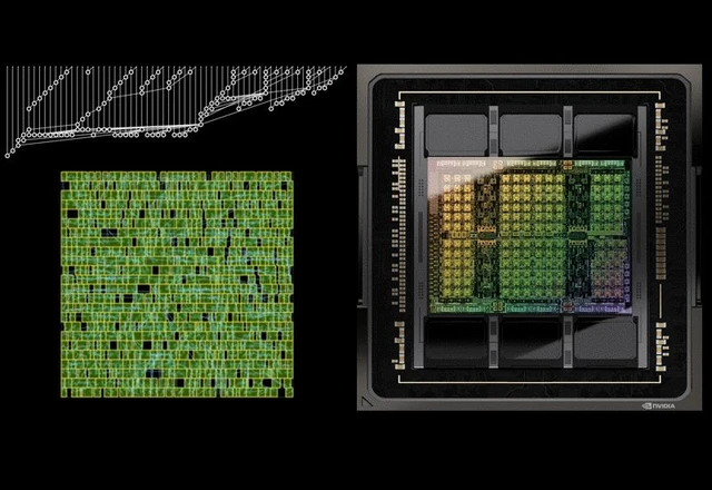
In the contemporary pursuit of computational supremacy, two fundamental philosophies of processor design have emerged. On one side are Intel and AMD, who are aggressively implementing multi-die architectures (chiplets) to integrate several smaller dies into a single system. On the other is Nvidia, which for a long time prioritized monolithic dies, striving for maximum integration of all components on a single silicon wafer. However, it is precisely this strategy that is now facing sharp criticism from experts at Huawei Technologies.
The core issue is that the infinite scaling of monolithic structures and the expansion of High Bandwidth Memory (HBM) inevitably hit a physical ceiling. Once a die reaches a critical size, manufacturing defect rates spike and heat dissipation becomes an insurmountable challenge. According to Huawei specialists, Western developers—relying heavily on advanced lithography—are heading toward a "cascading collapse," where further increases in physical chip size will cease to yield performance gains and instead lead to system degradation.
For Huawei, this is not merely a theoretical debate but an existential imperative. Due to stringent sanctions imposed by the US and its allies, the Chinese giant has been denied access to the latest Extreme Ultraviolet (EUV) lithography scanners essential for producing ultra-fine process nodes. In response, the company has been forced to shift its focus from manufacturing capabilities toward intelligent architectural design.
Rather than attempting to shrink transistors to limits accessible only to Western foundries, Huawei is betting on the so-called "Tau scaling" law. This concept involves finding innovative ways to optimize data transmission between system components. A key element here is the principle of LogicFolding—a design methodology that accelerates information flow within the chip without requiring cutting-edge lithography. The first mobile processor built on these principles is expected to be unveiled in the near future.
This approach effectively represents a transition from quantitative resource accumulation to a qualitative shift in computational structure. This trend is further validated by recent breakthroughs in artificial intelligence: the example of DeepSeek has demonstrated that cutting-edge LLMs can be developed even under hardware constraints, provided that algorithms and energy expenditures are meticulously optimized. Huawei is designing its AI chips to ensure maximum throughput with minimal power consumption—a goal that requires far more rigorous design work but offers significant advantages during operation.
As a result of this geopolitical schism, the world is witnessing the birth of two parallel semiconductor industries. One relies on lithographic precision and physical scaling; the other on structural optimization and architectural ingenuity. These two ecosystems will evolve independently, establishing divergent standards for efficiency and performance within the global digital landscape.
 Forecasting Exponential Growth in Nvidia Shipments