The AI arms race has definitively migrated from the abstract realm of algorithms into the physical domain of silicon. Today, market hegemony is defined not merely by software sophistication, but by the ability to guarantee an uninterrupted supply of massive computational power. The strategic alliance between Samsung and Broadcom represents a calculated response to this paradigm shift, forging a new axis of influence within the semiconductor landscape. This partnership is designed to fundamentally reshape the balance of power among the dominant architects of the global chip market.
The strategic alliance between Samsung Electronics and Broadcom—projected to exceed $200 billion in cumulative value by 2030—is far more than a mere commercial agreement; it is a long-term blueprint for the restructuring of AI infrastructure. This figure reflects the aggregate volume of investments and orders over several years, underscoring the colossal scale of resources required to maintain technological leadership in the era of generative models.
At the heart of this synergy lies the development of next-generation Application-Specific Integrated Circuits (ASICs), leveraging Samsung Foundry’s sub-2nm process nodes. In the semiconductor industry, breaking the 2-nanometer barrier necessitates a fundamental shift in current management—specifically through Gate-All-Around (GAA) architecture—which drastically reduces power consumption while simultaneously boosting transistor density. For Broadcom, this represents an opportunity to engineer chips with unprecedented performance; for Samsung, it is a chance to validate the efficacy of its cutting-edge lithography capabilities within high-load, real-world systems.
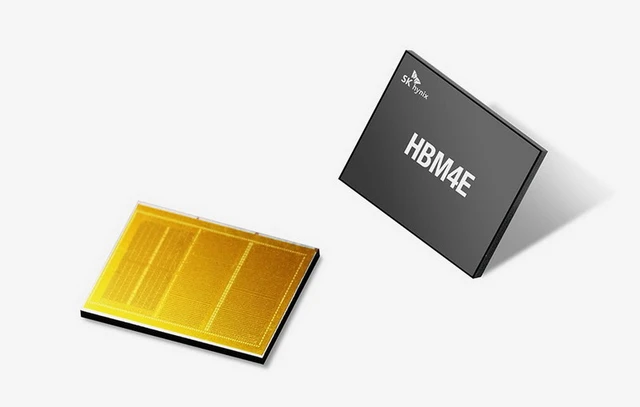
Parallel to advancements in logic computing, both parties are targeting the primary bottleneck of modern AI accelerators: memory bandwidth. The joint development of next-generation High Bandwidth Memory (HBM) aims to minimize latency between storage and the compute core. In this segment, Samsung is locked in a fierce competition with SK hynix, and Broadcom's backing could prove decisive in the battle to define memory standards for future generations of neural processing units (NPUs).
Significant emphasis is also being placed on Advanced Packaging technologies. The current industry pivot toward chiplets and 3D stacking effectively erases the boundary between the processor and volatile memory by integrating compute dies and memory modules into a single package. This approach allows for an exponential increase in data exchange speeds and a reduction in thermal output—factors that are critical for data centers, where hardware density is constantly increasing.
From a geopolitical and market-strategy perspective, this alliance represents a concerted effort to establish a viable alternative to TSMC’s hegemony in the contract manufacturing space. Samsung seeks to diversify its client base by attracting giants like Broadcom to ensure full fab utilization and accelerate the iteration cycle of its new process nodes.
It is telling that the partnership was unveiled in Silicon Valley during a visit by South Korean President Lee Jae-myung. This underscores that AI hardware development has evolved beyond corporate interests into a matter of national strategic priority. The synchronization of South Korean manufacturing prowess with American chip design expertise is forging a new industry standard, where success depends on the deep integration of every stage: from silicon design to final packaging and memory delivery.

 Power and Poise: The Xiaomi Pad 9 Pro Max