In the current geopolitical climate, semiconductors have emerged as the definitive strategic resource of the 21st century, elevating access to fabrication equipment to a critical matter of national security. Facing intensifying pressure from Western regulators, China is pivoting toward a strategy of absolute technological sovereignty, aiming to establish a fully autonomous semiconductor ecosystem. At the heart of this transition is AMEC, which seeks to secure dominance over the domestic market for advanced systems. This battle for hardware supremacy will ultimately dictate the global balance of power in electronics.
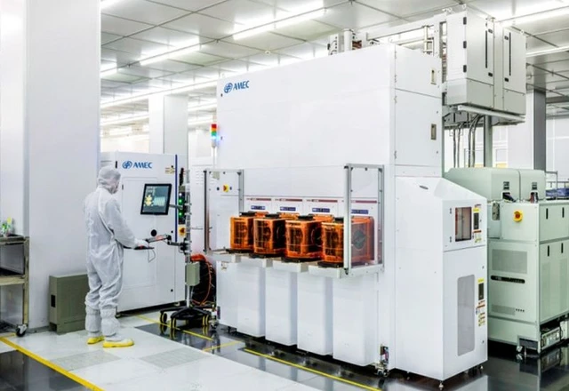
The fabrication of modern semiconductors represents one of the most intricate engineering feats in human history. It comprises hundreds of sequential stages, each requiring specialized equipment capable of extreme precision. Faced with external constraints, China's industrial sector has been forced to urgently restructure its supply chains. AMEC has emerged as the primary architect of this import substitution strategy, aiming to capture up to 60% of the domestic market for advanced equipment within the next five years.
Such a scale of expansion would effectively position AMEC as one of the world's largest providers of lithography and ancillary equipment. This trajectory is fueled by the colossal volume of chip production within the PRC, which has begun to dominate other regions in terms of sheer scale—with the exception of the most advanced leading-edge nodes concentrated in Taiwan and the US. To achieve its objectives, the company is radically expanding its technological ecosystem, planning to increase its product portfolio to over 100 different system types. Particular emphasis is being placed on mission-critical processes: plasma etching and thin-film deposition—the very operations that define the physical architecture and functionality of every transistor.
AMEC’s strategy is built on a long-term horizon extending to 2035, by which time the company intends to solidify its status as a global leader in terms of competitiveness and production scale. The growth dynamics are striking: over the past 14 years, the company's installed base has expanded by more than 35% annually. The economic efficiency of the business is further evidenced by high revenue per employee, which has reached $650,000.
This investment surge is underpinned by aggressive funding for research and development. Last year, AMEC allocated over 30% of its revenue to R&D, amounting to $554 million. Parallel to this, a massive expansion of manufacturing capacity is underway; this year alone, 600,000 square meters of new facilities are being commissioned across five different locations in China. Over the next five years, the pace of construction is expected to increase by another 50%, with annual capital expenditures on new capacity totaling at least $1 billion.
The company's technological progress is already manifesting in tangible shipments. By the end of last year, AMEC delivered over 6,800 process chambers for silicon wafer etching, spanning more than 20 market segments. A pivotal achievement is the equipment's ability to operate across process nodes ranging from 65nm down to 3nm, bringing the company closer to the bleeding edge of the global semiconductor industry. Financial results validate this strategy: revenue grew by 37% to $1.8 billion, while net profit increased by 31% to $313 million.
However, despite impressive strides in etching and deposition, a fundamental challenge remains for China's industrial push. In the segment of lithographic scanners—the most complex machines in chip production—local manufacturers still lag several generations behind global leaders. Closing this gap will require not only time and capital but genuine scientific breakthroughs. Nevertheless, AMEC’s systemic approach and the overall momentum of Chinese industry suggest that technological dependence on foreign suppliers is gradually becoming a relic of the past.
 Forecasting Exponential Growth in Nvidia Shipments