The global AI race has pushed the industry toward a critical impasse: traditional data transfer methods between processors and memory have become a systemic bottleneck. Modern neural networks demand more than just expanded capacity; they necessitate a fundamental reimagining of the very physics governing component interaction. Samsung is addressing this challenge with a new technological roadmap, one where the boundaries between storage and computation are beginning to dissolve. This transition heralds an era of deep structural integration, engineered to overcome the escalating energy and thermal crises plaguing today's data centers.
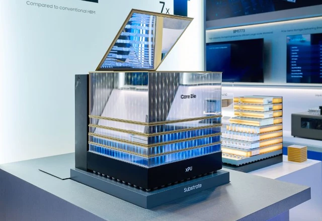
The evolution of high-performance memory has reached a tipping point where incremental generational leaps in HBM are no longer sufficient. In response to this challenge, Samsung is introducing the zHBM concept—a technological leap promising an eightfold increase in performance over the upcoming HBM5 standard and a tenfold surge in data density.
The key to these metrics lies in the physical architecture: rather than the conventional planar layout on a shared interposer with the GPU, zHBM envisions mounting the memory stack directly onto the GPU die. This radically shortens the signal path and minimizes latency. By leveraging advanced wafer-to-wafer bonding, Samsung can implement tens of thousands of data channels within a single stack. Combined with significantly improved thermal management—reducing thermal resistance by more than half—and a threefold increase in energy efficiency, zHBM provides the ideal foundation for the next generation of AI accelerators. Furthermore, Samsung envisions the integration of custom logic directly into the memory stack, allowing clients to tailor the hardware to the specific requirements of their proprietary algorithms.
Parallel to this, the HBM5 standard is evolving as a critical intermediate stage. Projections suggest it will deliver double the bandwidth of HBM4E. The primary focus here is thermal regulation; the implementation of advanced cooling systems is expected to reduce thermal resistance by 20%, which is critical for preventing thermal throttling under extreme workloads. The foundation for these innovations is already in place: Samsung has commenced mass production of HBM4 utilizing a 4nm base die and 10nm-class (1c) DRAM, with HBM4E samples already being deployed to key partners.
In the realm of long-term storage for AI computing, the strategy centers on zNAND-O, based on V-NAND architecture. The primary objective is the near-total elimination of latency when moving data between adjacent system nodes. The previously introduced Z-NAND concept sets ambitious targets: a 15-fold increase in performance and an 80% reduction in power consumption. While the cost of such a solution may be up to four times higher than traditional TLC NAND, this compromise is justified for high-load AI systems where access speed is the primary currency.
The evolution of V-NAND also warrants particular attention. The new V10 BV-NAND generation has breached the 400-layer threshold, made possible by innovative interlayer connection technology. Compared to its predecessor (V9), data storage density has increased by 58%, with marked improvements in read and write speeds. This technology has drawn significant interest from Nvidia, as it allows for a substantial increase in memory capacity within a constrained physical footprint. The upcoming V11 generation is expected to hit the 500-layer mark, effectively turning the memory chip into a "silicon skyscraper."
Completing this architectural shift is the transition toward the PIM (Processing-In-Memory) paradigm, implemented in LPDDR5X-PIM. The traditional von Neumann architecture—where data constantly shuttles between memory and the processor—creates massive energy overhead and temporal lags. Samsung’s solution allows a portion of computational operations to be executed directly within the memory itself. This not only accelerates data processing but also radically reduces the load on the central processor, optimizing the power efficiency of the entire system.
 Breaking the Lithography Barrier in China