The modern semiconductor industry is rapidly converging upon the physical limits of silicon scaling. This quest for viable alternatives has led researchers toward two-dimensional (2D) materials, which promise a drastic reduction in both power consumption and device footprints. However, the primary bottleneck hindering commercialization has remained the inherent instability of the interfaces between semiconductors and insulators. A breakthrough proposed by TSMC engineers and Taiwanese scientists pivots the strategic focus away from the mere discovery of new materials toward the precision engineering of atomic layers.
The era of silicon-based electronics is steadily colliding with the fundamental constraints of physics. As transistor dimensions approach the atomic scale, parasitic effects begin to dominate, rendering current control highly inefficient. In this context, molybdenum disulfide ($\text{MoS}_2$) has emerged as a primary contender to succeed silicon. Its chief advantage lies in its two-dimensional structure: a material layer only about 0.7 nm thick allows for far more effective suppression of short-channel effects, which become critical during the extreme scaling of logic elements.
However, the transition from laboratory prototypes to actual chip production has encountered a significant technological bottleneck: the creation of a high-quality gate insulator. The surface of a 2D $\text{MoS}_2$ crystal is virtually devoid of dangling chemical bonds, making it "smooth" from a chemical perspective. Consequently, standard industrial methods—specifically Atomic Layer Deposition (ALD)—perform poorly under these conditions; continuous and uniform ultrathin films fail to form on the surface, leading to defects and current leakage.
The situation was further complicated by the use of high-k dielectrics, such as hafnium oxide ($\text{HfO}_2$). While effective for charge management, these materials trigger intense electron scattering, which drastically reduces carrier mobility. Engineers faced a classic dilemma: either ensure high current controllability at the expense of transistor speed, or maintain carrier mobility while accepting poor gate control and high defect rates.
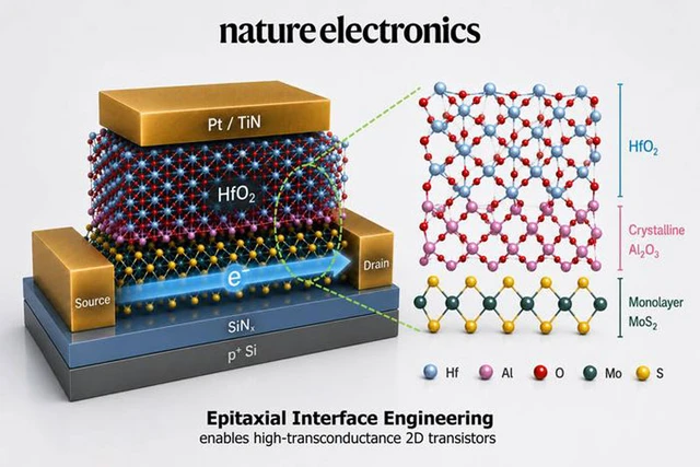
The breakthrough occurred when researchers shifted their focus from searching for the "ideal" material to engineering the ideal interface between them. The solution was the introduction of an atomically thin buffer layer that functioned not merely as a mechanical spacer, but as an active component of the transistor.
Under ultra-high vacuum conditions, a layer of aluminum approximately 0.3 nm thick was deposited onto the $\text{MoS}_2$ surface using electron-beam evaporation. Due to the specific nature of van der Waals interactions in 2D materials, the aluminum crystallized with a specific $\text{Al}(111)$ orientation. Subsequent controlled oxidation transformed this layer into an exceptionally thin and uniform film of aluminum oxide ($\text{Al}_2\text{O}_3$). Only after this step was the primary dielectric, $\text{HfO}_2$, applied via ALD.
This multilayer stack solved two problems simultaneously: it provided a suitable foundation for the growth of a high-quality dielectric and shielded the channel from the adverse effects of hafnium oxide.
The results were impressive. In the resulting short-channel transistors, researchers managed to reduce the equivalent oxide thickness (EOT) of the gate dielectric to 1 nm while maintaining high carrier mobility. This synergy resulted in exceptional transconductance—the key performance metric for any transistor.
While this work serves more as a demonstration of a technological principle than a ready-made replacement for standard CMOS structures, it proves a critical thesis: the barriers to two-dimensional electronics are surmountable. The path to the next generation of processors lies in interface engineering at the atomic level, where the boundaries between materials become tools for manipulating the physical properties of the device.
 Next-Generation Ultra-Lightweight Lens Technology