Modern mobile devices are rapidly evolving into full-scale computing workstations, where the local execution of neural networks demands immense memory bandwidth. Legacy storage standards have become a critical bottleneck, throttling the potential of today's most powerful processors. Samsung’s response—the UFS 5.0 standard—represents a quantum leap, blurring the line between mobile storage and high-performance desktop SSDs. This technology lays the groundwork for a new generation of AI-driven smartphones capable of processing massive datasets with unprecedented velocity.
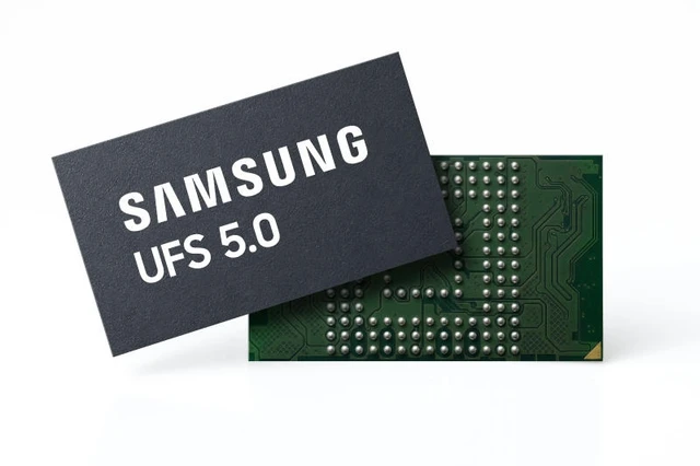
The mobile technology landscape has shifted into an era where raw CPU clock speeds are no longer the sole arbiter of performance. Today, the critical bottleneck has moved to the data throughput between storage and RAM, particularly as On-Device AI matures. Samsung's debut UFS 5.0 prototype delivers staggering benchmarks: sequential read speeds of 10.8 GB/s and write speeds of 9.5 GB/s.
To put this technological leap into perspective, one only needs to look at the current UFS 4.1 standard. The preceding generation topped out at read and write speeds of 4,300 and 4,100 MB/s, respectively. This represents more than a twofold increase in bandwidth. Such a performance surge translates directly into a superior user experience: cold-boot times for resource-intensive applications are virtually eliminated, and the execution of local Large Language Models (LLMs) and generative AI becomes nearly instantaneous, as the latency involved in loading model weights from non-volatile memory is reduced to a critical minimum.
In the mobile sector, however, raw speed is never the sole priority. Thermal management and battery longevity remain the primary engineering hurdles. Samsung has addressed these constraints through aggressive power optimization, achieving a 40% reduction in energy consumption compared to UFS 4.1. This was realized via the implementation of clock gating mechanisms—which deactivate idle portions of the chip—and a transition to multi-level voltage regulation. The result is desktop-class performance without compromising mobile autonomy.
Miniaturization remains the hallmark of mobile architecture. The new chip maintains an ultra-compact footprint of 7.5 × 13 × 0.9 mm, enabling integration into ultra-slim chassis or freeing up precious internal volume for larger batteries. UFS 5.0 is expected to be a cornerstone of the next-generation flagship ecosystem, working in synergy with the upcoming Exynos 2700 processor—the rumored heart of the Galaxy S27 series.
The transition of this technology to the consumer market will not be instantaneous. Mass production of these next-gen drives is slated for the fourth quarter of 2026. Initial modules will offer capacities up to 1 TB, which, coupled with unprecedented speeds, will transform smartphones into legitimate professional workstations for content creation and complex edge computing, right in the user's pocket.
 A New Memory Paradigm for AI Accelerators