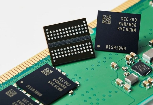
The current AI surge is placing unprecedented pressure on hardware, positioning memory speed and reliability as the primary bottlenecks in modern computing architectures. Consequently, the global semiconductor industry has pivoted toward discovering materials that can marry energy efficiency with extreme endurance—specifically, a massive rewrite cycle capacity. Ferroelectrics have emerged as the critical catalyst in this pursuit, promising to blur the distinction between volatile (RAM) and non-volatile storage. A recent technological breakthrough in this field has extended storage lifespan by a hundredfold, paving the way for the development of ultra-stable, enterprise-grade server solutions.
The pursuit of the ideal memory architecture is fundamentally a search for materials with an optimal crystalline structure. Researchers are particularly focused on wurtzite-structured ferroelectrics, among which scandium-doped aluminum nitride (AlScN) has emerged as a frontrunner. This material possesses critical performance characteristics: exceptionally low power consumption and high switching speeds. Furthermore, AlScN is fully compatible with existing semiconductor fabrication processes, making its integration into mass production economically viable.
However, the path to practical application was long obstructed by the hurdle of physical degradation. Previous iterations of AlScN-based chips exhibited unsatisfactory reliability, with devices failing after approximately 100 million write cycles. For modern data processing systems, where rewrite operations occur billions of times per second, such a lifespan is catastrophically insufficient.
The key to solving this problem lay in a granular analysis of processes occurring at the atomic level. Researchers discovered that premature failure was caused by lattice defects—specifically, the absence of nitrogen atoms, known as vacancies. While these defects were not inherently fatal, they began to migrate during the state-switching process. Over time, these nitrogen vacancies clustered together, forming microscopic conductive channels. These channels facilitated current leakage, which inevitably led to material degradation and the ultimate failure of the chip.
For years, the industry had documented the fact of device failure, but the underlying mechanisms remained purely hypothetical. Understanding exactly what was moving within the structure—and how this movement triggered a systemic collapse—allowed scientists to move from merely observing the problem to eliminating it.
The newly engineered material structure effectively inhibits the migration and aggregation of nitrogen vacancies. By creating a structural barrier to defect movement, the formation of conductive channels was prevented. The result was striking: the write endurance increased to 10 billion cycles.
This quantum leap shifts the trajectory of server hardware evolution. If this technology can be scaled to an industrial level, we will gain a type of memory that combines the speed of RAM with the non-volatility of Flash storage, while possessing the durability required for the most demanding neural network training tasks and high-throughput AI systems.
 Forecasting Exponential Growth in Nvidia Shipments