The semiconductor industry is currently pivoting from monolithic dies toward modular architectures, with manufacturing costs emerging as the primary constraint. In its latest mainstream offerings, Intel is striving to strike a delicate balance between cutting-edge performance and economic viability. Project Wildcat Lake has served as a testing ground for a radical reimagining of how to streamline premium design without compromising the end-user experience. At the core of this strategy lies a complex technical trade-off between packaging costs and data interconnect efficiency.
The development of the Core Series 3 (Wildcat Lake) mobile processors was not an attempt to pioneer a fundamentally new product. Instead, Intel's engineers were tasked with a delicate "surgical" refinement of the existing Panther Lake design. The objective was a selective reduction in costs without sacrificing the functionality critical to the average user. This strategy rested on three fundamental pillars: replacing expensive packaging, optimizing functional blocks, and implementing a specialized inter-chip interconnect.
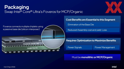
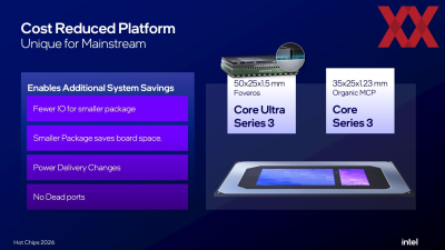
The centerpiece of this transformation was the move away from Foveros technology. In premium Core Ultra 3 chips, a passive base die (silicon interposer) is used to integrate several chiplets into a single structure. However, for the mass market, such complexity is prohibitively expensive and increases assembly defect rates. The solution was a transition to an organic Multi-Chip Package (MCP). This shift significantly streamlined the manufacturing process and lowered the per-unit cost.
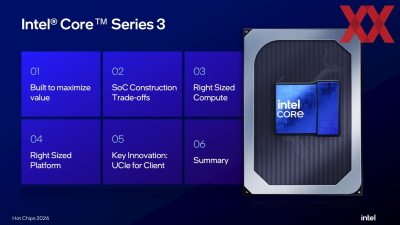
The shift to MCP brought about tangible physical changes. The package dimensions were reduced from 50 × 25 × 1.5 mm to 35 × 25 × 1.23 mm. This compact footprint not only saves precious real estate on the motherboard but also optimizes power delivery by eliminating "dead" contacts. However, simplifying the packaging introduced new challenges: without the interposer, the number of signal paths was drastically reduced, necessitating a complete overhaul of the power management system.
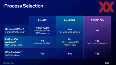
To maintain computational power, Intel continued to utilize the 18A process node for high CPU core efficiency, while the I/O block (Thunderbolt, USB, PCIe) was fabricated using TSMC's N6 node. To bridge these heterogeneous dies, Intel opted for the UCIe (Universal Chiplet Interconnect Express) standard.
The implementation of UCIe was a necessary compromise to offset the absence of the Foveros base die. The primary hurdle here was interconnect density: the bump pitch increased from 36 $\mu$m to 110 $\mu$m. To compensate for the loss in pin density, engineers had to increase data transmission speeds. Consequently, the area occupied by inter-chip connections grew by approximately 70%. Intel deemed this trade-off justified, as the overall cost of MCP packaging remained significantly lower.
The technical execution of UCIe encountered several serious obstacles. First, protocol conflicts emerged: packetized data transmission created latencies that clashed with slow sideband signals. Synchronizing data with control signals during boot-up and debugging became one of the most complex tasks of the entire project. Second, power consumption increased due to the need to maintain a constant bus frequency to avoid idle states, particularly during video signal transmission. To mitigate this, specialized channel states and Quality of Service (QoS) traffic prioritization were implemented.
The third critical concern was signal integrity. At high frequencies, UCIe exhibits sensitivity to voltage fluctuations and Bit Error Rates (BER). To avoid the cost of expensive LDO (Low-Dropout) regulators, Intel capped the data transfer rate at 8 Gbps and eschewed retry mechanisms in favor of a conservative reduction in frequency.
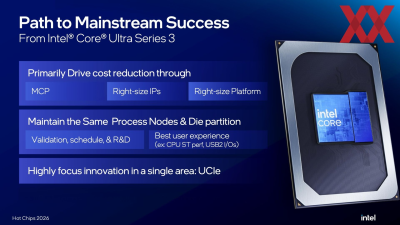
Parallel to the packaging changes, a rigorous optimization of computing resources was undertaken. To reduce die area, Intel employed a method of "radical pruning":
- The Xe graphics subsystem was scaled down from four cores to two, with ray tracing support being completely removed.
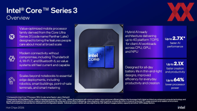
- The Neural Processing Unit (NPU) was reduced from three cores to one, dropping performance from 53 to 17 TOPS.
- The number of performance P-cores was cut from four to two, and the L3 cache was halved from 12 MB to 6 MB. Despite this, single-threaded performance was preserved.
- The Image Processing Unit (IPU) was removed entirely, with camera functions migrated to the USB2 ISP.
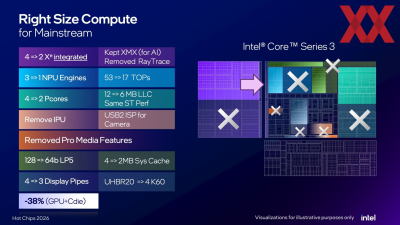
These measures reduced the area of the compute and graphics dies by 38%. The I/O block also underwent optimization: the number of Thunderbolt/USB4 ports was reduced to two, and the memory interface was scaled down from 128-bit to 64-bit LP5. Collectively, this resulted in a 15% reduction in the I/O block's footprint.
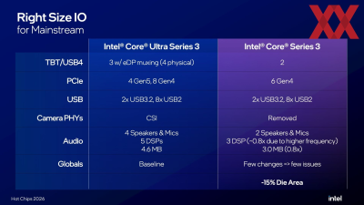
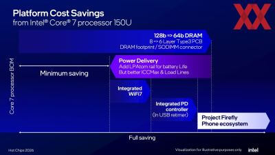
The effects of this optimization extended to the platform level. The transition to 64-bit memory allowed the PCB layer count to be reduced from eight to six, significantly lowering laptop manufacturing costs. Furthermore, the direct integration of the Wi-Fi 7 module and the Power Delivery controller into the system improved battery life and increased the overall capacity of the power delivery system.
Ultimately, Wildcat Lake demonstrates a pragmatic approach to product development. By leveraging advanced process nodes and a modular architecture, Intel has created an accessible solution that preserves the core user experience while maximizing the efficiency of every square millimeter of silicon.
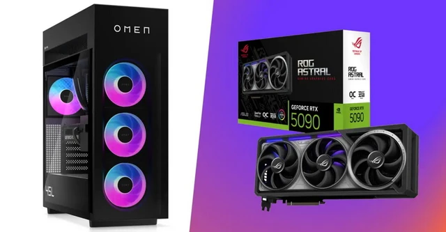 The Economic Paradox of the GeForce RTX 5090