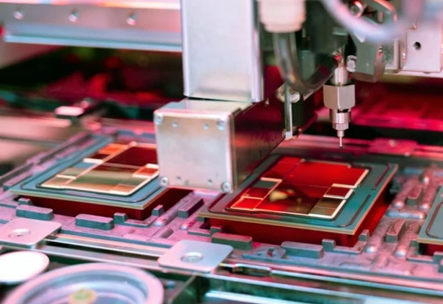
In the current arms race for AI compute, memory bandwidth has emerged as the primary bottleneck. While traditional HBM solutions deliver staggering speeds, they demand intricate and costly semiconductor-level integration. The introduction of JEDEC’s SPHBM4 standard is poised to shift this paradigm, offering an alternative trajectory toward high performance. The industry now possesses a mechanism to drastically lower manufacturing costs without compromising on raw data throughput.
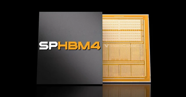
In the realm of high-performance computing (HPC), the battle is fought not only over transistor counts but over the efficiency of data delivery to the processor. JEDEC, the global authority on memory standards, has introduced the JESD330-4 specification, detailing SPHBM4 (Standard Package High Bandwidth Memory). This standard aims to resolve one of the most pressing challenges in modern electronics: the prohibitive cost and complexity of integrating memory stacks with the compute core.
The pivotal innovation of SPHBM4 lies not in the architecture of the DRAM dies themselves—which remain identical to those used in conventional HBM4—but in a radical overhaul of the base layer interface. Traditional HBM4 implementations rely on a massive interface featuring 2,048 data signals, demanding extreme mounting precision and the use of costly silicon interposers to facilitate communication between the memory and the SoC. SPHBM4 disrupts this approach by reducing the number of signal lines to 512.
At first glance, such a reduction might seem like a regression; however, the deficit in physical lines is offset by an increase in interface clock speeds and the implementation of a 4:1 data transmission sequence. Essentially, each individual contact now transmits four times more information per unit of time. Consequently, aggregate throughput remains on par with HBM4, while the physical realization of the interconnect becomes significantly simpler.
This engineering pivot paves the way for the adoption of traditional organic (PCB) substrates over expensive silicon solutions. Increasing the pitch between micro-contacts reduces positioning precision requirements and lowers manufacturing defect rates. Furthermore, organic substrates allow for longer interconnect traces between the processor and memory. For accelerator developers, this means the ability to deploy a greater number of memory stacks around the SoC die, directly increasing total system capacity without a proportional spike in cost.
It is critical to understand that SPHBM4 is not a wholesale replacement for HBM4 in its classical sense. Rather, it represents an alternative methodology for packaging and component interaction within a single module. The JESD330-4 standard offers flexibility: developers can now choose between maximum interconnect density (classic HBM4) and economic optimization while maintaining the same data transfer rates (SPHBM4).
While JEDEC has yet to disclose specific implementation timelines or a roadmap of the first products to support SPHBM4, the formalization of this approach signals an industry-wide drive toward making high-performance memory more accessible and scalable. This shift is absolutely critical for the continued evolution of large language models (LLMs) and complex neural network infrastructures.
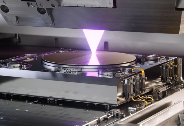 The Horizon of China's Technological Sovereignty in Lithography