The global race for smaller nodes has evolved beyond a mere contest of engineering prowess; it is now a test of financial stamina. The deployment of High-NA (high numerical aperture) scanners promises a quantum leap in transistor density, yet the cost of such advancement is reaching a critical threshold. While some industry titans double down on aggressive technological leaps, others are forced to strike a precarious balance between ambition and profitability. At the epicenter of this struggle stands Samsung, whose trajectory toward 2nm silicon is now being dictated by harsh economic realities.
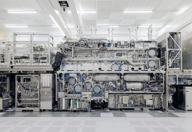
In modern microelectronics, the race for transistor density has pushed standard Extreme Ultraviolet (EUV) lithography to its physical limits. The solution lies in High-NA—High Numerical Aperture lithography—which enables finer resolution and reduces the number of exposure passes. However, this technological leap requires staggering capital expenditures, positioning ASML's equipment as some of the most expensive tools in industrial history.
Samsung Electronics has already made its initial foray into this territory, deploying two cutting-edge High-NA scanners at its Hwaseong facility for experimental purposes. The total expenditure for these acquisitions is estimated to exceed $670 million. Despite technical readiness, the company remains cautious about scaling the technology. The primary driver is the financial health of its foundry business, which has remained unprofitable since 2022. As the division strives to return to profitability by the end of the current year, massive investments in High-NA could become an unsustainable burden and lead to further financial losses.
From a technical standpoint, Samsung's progress remains impressive. The current yield rate for its 2nm chips has reached 55%. In the semiconductor industry, there is an implicit threshold of 60% beyond which production is considered commercially viable for mass manufacture. While Samsung could technically implement High-NA EUV immediately to optimize the process and reduce manufacturing steps, economic pragmatism dictates a different path: first stabilize profitability and expand its pool of major clients before committing to a costly fleet upgrade.
The current market landscape highlights a stark divergence in the strategies of the three primary players. Intel has opted for an aggressive pursuit of leadership, already integrating High-NA EUV into the production of its Panther Lake mobile processors under the Intel 18A node. This is a calculated move by the American giant to reclaim technological supremacy through the rapid adoption of next-generation tooling.
At the opposite end of the spectrum is TSMC. The Taiwanese market leader maintains a distinctly conservative stance, planning full-scale High-NA implementation no earlier than 2029. Leveraging its massive scale and the efficiency of current methods, TSMC intends to maximize the lifespan of standard EUV systems. Internal roadmaps suggest that upcoming A12 and A13 nodes can bypass high-numerical aperture scanners, although the company continues to acquire them for research purposes to avoid a future technological dead end.
Consequently, the industry is entering a phase where the critical metric is no longer just the ability to achieve a certain density, but the cost of producing it. Samsung finds itself in the most precarious position, attempting to balance its ambitions for cutting-edge 2nm components with the urgent need to restore its financial health.
 Nvidia N1X and the New Era of Arm PCs