The relentless pursuit of semiconductor miniaturization has collided with the fundamental boundaries of materials science. As feature sizes shrink toward the atomic scale, conventional dielectrics lose their ability to effectively isolate signals. Today, the primary technical bottleneck has shifted toward mitigating parasitic capacitance and metal diffusion within ultra-dense architectures. Emerging research into amorphous carbon is paving the way for a new generation of stable, high-performance insulators—a breakthrough that TSMC, the Taiwanese semiconductor powerhouse, is already evaluating for integration into high-volume manufacturing.
For decades, the roadmap for computing has followed a straightforward premise: smaller transistors equate to higher performance and greater energy efficiency. However, this trajectory has led the industry to an "atomic barrier," where the fundamental properties of materials begin to warp. At these scales, electrical signals become erratic, and the dielectrics intended to provide isolation lose their efficacy.
One of the most critical bottlenecks in modern processor design is not the size of the transistor itself, but the complexity of the interconnect system. Billions of components are linked by ultra-fine copper conductors packed so densely that parasitic capacitance emerges. This leads to crosstalk between adjacent lines, inevitably driving up power consumption and throttling data transmission. Combating this effect requires low-k (low dielectric constant) materials, but existing porous insulators become mechanically unstable and impractical when thinned down to a few nanometers.
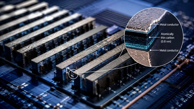
A potential resolution to this dilemma lies in the use of ultra-thin amorphous carbon films dominated by sp2 bonds. Researchers at the National University of Singapore have developed a material just 0.8 nm thick that exhibits a unique combination of physical properties. Its dielectric constant is approximately 1.35—strikingly close to that of a vacuum (1.0). Simultaneously, the film can withstand electric fields of 28–31 MV/cm, surpassing even promising alternatives like amorphous boron nitride.
The mechanical resilience of this solution is particularly noteworthy. The hardness of the carbon layer reaches 100 GPa, roughly an order of magnitude higher than traditional silicon dioxide. This enables the creation of ultra-thin yet structurally robust barriers that remain intact during chip fabrication and operation.
Beyond insulation, amorphous carbon effectively addresses the challenge of metal migration. In modern microelectronics, tantalum nitride is typically used to prevent copper from leaching into adjacent layers, though it consumes significant real estate. The new carbon layer serves a dual purpose: it acts as a low-k dielectric while simultaneously functioning as a diffusion barrier against metal ions. Tests indicate that even at 0.8 nm, this material is a hundred times more effective at blocking metal migration than the widely used tantalum nitride.
The technological potential of this breakthrough is amplified by its ease of integration. The film is produced via Chemical Vapor Deposition (CVD) at relatively low temperatures (around 300°C). Crucially, the material can uniformly coat not only flat surfaces but also complex geometries and recesses. This opens significant possibilities for 3D element stacking, a pivotal trend in the evolution of the semiconductor industry.
Currently, the technology remains in the laboratory phase, utilizing small-diameter wafers. However, the transfer of data to TSMC engineers signals strong commercial potential. The primary hurdle remains scaling the process for industrial volumes; yet, if adaptation succeeds, the industry will gain a powerful tool to push past the physical limits of miniaturization.
 Starship's Return from the Indian Ocean