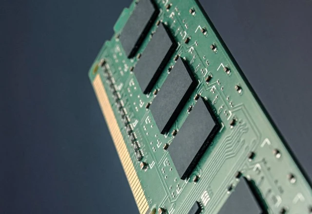
The global AI surge has ignited an unprecedented demand for high-performance memory, elevating it to one of the most critical strategic assets in the modern economy. Amidst escalating geopolitical volatility, the localization of manufacturing has emerged as the primary mechanism for ensuring supply chain resilience and safeguarding technological sovereignty. South Korean industry titan SK hynix is making a strategic pivot, relocating a portion of its production capabilities directly to U.S. soil. The establishment of a massive HBM packaging facility in Indiana is designed to cement the company's dominance in the age of neural networks.
For years, the footprint of South Korean players in the U.S. semiconductor market remained constrained, primarily centered on Samsung Electronics' foundry services for logic components. However, current market dynamics demand deeper integration. SK hynix intends to radically reshape this landscape, transforming its new Indiana facility into the largest High Bandwidth Memory (HBM) packaging hub in the United States. The ambition is clear: by 2030, outpace local incumbent Micron Technology and become a cornerstone of the U.S. data infrastructure.
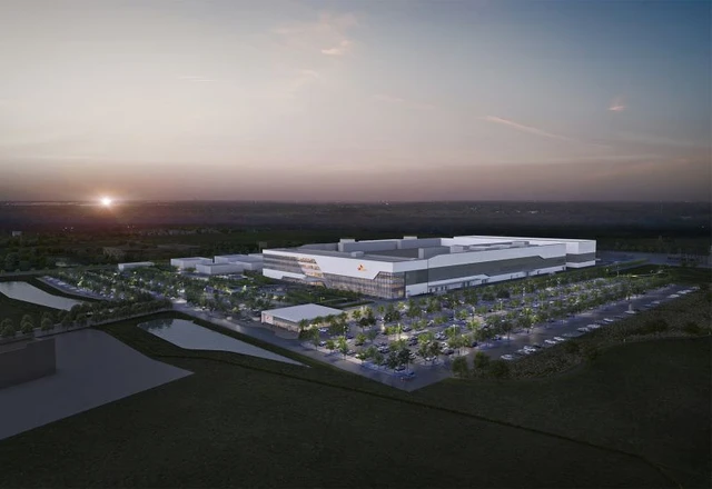
The project involves a $4 billion investment, though the facility's architecture is specialized. Rather than full-scale wafer fabrication, the Indiana plant will focus on the final stages: testing and packaging. The semiconductor wafers themselves will be shipped from South Korea, allowing the company to keep its proprietary lithography processes onshore while establishing a physical product presence within the U.S. According to the roadmap, the complex's first cleanroom will open in October 2028, with full-scale serial production of next-generation memory slated for the second half of 2029.
The fiscal viability of this maneuver is underpinned by the company's staggering success on the public markets. A recent U.S. listing enabled SK hynix to raise $26.5 billion, a record for foreign issuers. This rapid surge in capitalization—now exceeding $1 trillion—provides the necessary capital for aggressive expansion. While the company remains committed to expanding capacity within South Korea, domestic infrastructure bottlenecks are forcing it to seek new frontiers abroad.
Integration into the Indiana economy will be comprehensive. Beyond creating 1,000 permanent jobs and 6,000 positions during the construction phase, the company is betting on strategic academic alliances. Purdue University will spearhead the cultivation of specialized talent and joint R&D initiatives, evolving the facility from a mere manufacturing node into a full-fledged R&D center. Initially, operations will be led by veteran specialists from Korea, who will gradually transition management to local engineers.
By 2030, SK hynix's total investment in the U.S. industry is expected to surpass $45 billion. These funds will be allocated not only to the Indiana site but also to the development of its AI Company and Solidigm—the unit acquired from Intel in 2020, which bolstered SK hynix's position in the NAND flash market. The government is actively fueling this transition: federal subsidies will total $458 million, with state-level support adding another $712 million, marking one of the most significant incentive packages in the region's history.
The strategic imperative of this venture extends beyond simple manufacturing. Establishing research laboratories directly within the U.S. will allow for the rapid tailoring of memory specifications to meet the demands of Tier-1 clients. A prime example of this synergy is the $500 billion deal with Nvidia, which envisions close cooperation in developing novel memory architectures. Within the current semiconductor hierarchy, SK hynix already holds the title of global leader in the HBM segment; its U.S. expansion is designed to cement this dominance, even as Samsung maintains a lead in overall memory market share.
 Nvidia’s Technological Pragmatism in the Open-Model Race