The semiconductor industry has reached the limits of traditional lithography, where every single nanometer of progress now demands staggering capital expenditure. Transitioning to High-Numerical Aperture (High-NA) EUV equipment has become the sole viable path for continuing the scaling of transistor density. Yet, this technological leap is unattainable without a fundamental overhaul of the core tooling—most notably, the dimensions of the photomasks. A global consensus among TSMC, Samsung, and Intel marks the beginning of a new era in chip fabrication, one where economic viability is now as critical as physical precision.
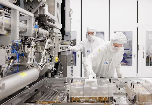
At the core of every modern microprocessor lies the process of photolithography—essentially a highly sophisticated form of "printing" microstructures onto a silicon wafer. This process relies on photomasks, which define the geometry of future circuits and allow them to be projected onto the die using ultraviolet radiation. For decades, the industry has relied on a 150mm mask size standard, but today, this standard is becoming a bottleneck, throttling throughput and driving up the cost of the final product.
Doubling the photomask size to 300mm is more than a mere technical adjustment; it is a strategic maneuver designed to optimize the entire production cycle. When paired with the latest High-NA (High Numerical Aperture) EUV scanners, which provide superior beam focusing precision, the transition to enlarged masks significantly increases line throughput. According to ASML, the world's primary supplier of lithography equipment, this synergy can boost scanner efficiency by 40% while simultaneously simplifying the design process for complex chips.
However, the deployment of High-NA EUV entails staggering capital expenditures. Each unit costs tens of millions of dollars, and adapting to the technology requires a complete overhaul of the factory infrastructure. This is precisely why the market's largest players have opted to synchronize their roadmaps. A collective transition to the new mask standard allows for the distribution of development costs and mitigates risks that might otherwise be prohibitive for a company acting alone.
The pace of adoption varies significantly across the three industry giants. Intel has positioned itself as the aggressive trailblazer; for over three years, the company has championed the shift to larger masks and has effectively moved from experimentation to the serial application of High-NA EUV. These systems are already being utilized in the production of the Panther Lake processor family under the Intel 18A process, granting the company a temporary strategic advantage in the race for transistor density.
Samsung intends to scale High-NA EUV by 2028, with memory production serving as the primary priority, as lithographic precision is critical for increasing cell capacity. Regarding the transition to new photomasks, the Korean giant is betting on close collaboration with industry partners to minimize overhead.
TSMC, the perennial market leader, is adopting a more measured and pragmatic stance. The Taiwanese giant plans to fully integrate High-NA EUV equipment into its production lines by 2030. Notably, in the initial phase, TSMC will continue using traditional 150mm masks to stabilize the process. A pilot line for 300mm masks will not be launched until 2031, with full-scale integration into serial chip production expected by 2033.
This divergence in timelines underscores the contrasting philosophies of these companies: from Intel’s drive for a technological leap at any cost to TSMC’s commitment to maximum optimization and reliability. Nevertheless, the general trajectory is clear. The transition to the 300mm standard and High-NA EUV is a necessary step to ensure that Moore's Law continues to hold, enabling the creation of more powerful and energy-efficient semiconductors amidst ever-growing demands for computational power.
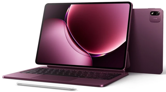 Power and Poise: The Xiaomi Pad 9 Pro Max