The relentless pursuit of smaller process nodes in the semiconductor industry has collided with a formidable barrier: the exponential surge in equipment costs. Modern Extreme Ultraviolet (EUV) lithography, which enables the fabrication of chips with staggering transistor densities, demands optical systems of unprecedented complexity. A groundbreaking study from the Okinawa Institute of Science and Technology proposes a radical reimagining of the fundamental geometry underlying these systems. Shifting toward a linear architecture could do more than just streamline the production of nanometer-scale structures; it could drastically lower the financial barrier to entry for the next generation of high-performance computing.
The modern high-tech landscape is fundamentally underpinned by Extreme Ultraviolet (EUV) lithography. With a wavelength of just 13.5 nm, this light allows engineers to "etch" features onto silicon that approach atomic scales. However, the physics of EUV radiation imposes brutal constraints: this light is absorbed by virtually every material, including the glass used in conventional lenses. Consequently, the entire optical system must operate within a deep vacuum, replacing traditional lenses with incredibly complex multilayer mirrors.
Current industrial scanners, which dominate the market, employ a highly sophisticated off-axis configuration. The beam traverses a system of mirrors, reflects off a photomask containing the circuit pattern, and is then focused onto the silicon wafer. To push resolution further, the industry is transitioning to High Numerical Aperture (High-NA) systems, which allow for the capture of a wider range of angles. Yet, increasing the NA inevitably exacerbates distortions and complicates the architecture, transforming each scanner into an engineering marvel costing hundreds of millions of euros.
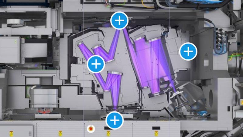
One of the primary hurdles developers faced as far back as the 1990s was the so-called "3D mask effect." Because light strikes the reflective mask at an angle, geometric distortions occur that cannot be fully eliminated through simple means. It was precisely this challenge that forced the industry toward the cumbersome and prohibitively expensive off-axis systems seen in today's installations.
An alternative approach, proposed by Professor Tsumoru Shintake, suggests a return to linear geometry. In his concept, the photomask, projection optics, and silicon wafer are aligned on a single axis. To circumvent the aforementioned distortions, he proposes a focusing system comprising two optical components, each consisting of a pair of concave and convex mirrors.
The core of this innovation lies in the precision calculation of the mirror profiles and the distance between them. Simulations indicate that multiple reflections within such a system can mutually compensate for a portion of the distortions while maintaining a high numerical aperture and flawless image quality. Essentially, the complex "optical labyrinth" is replaced by a more direct and predictable beam path, which should significantly simplify both the manufacturing and the subsequent calibration of the equipment.
The economic implications of such simplification could be colossal. Preliminary estimates suggest that equipment costs could drop by three to four times, paving the way for the mass production of 2–3 nm features. In the long term, this would lower the cost of high-density memory and logic circuits, directly impacting the cost of infrastructure required to train and support massive AI models and data centers.
Nevertheless, the road from theoretical model to industrial application remains fraught with challenges. Current calculations are based on the concept of ideal mirrors with one hundred percent reflectivity. In reality, every reflection in the EUV spectrum is accompanied by energy loss, and the requirements for mirror surface smoothness are measured in angstroms. The research team is now moving into the most critical phase: the creation of a physical prototype. If experimental data validate the calculations, the industry may find a way to break the current technological impasse, making the most advanced chips more accessible and energy-efficient.
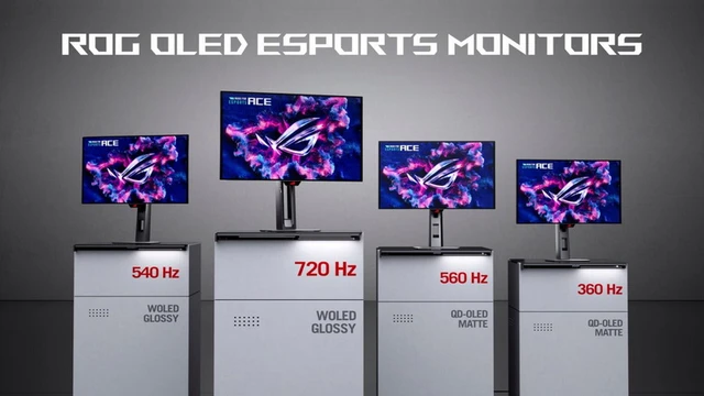 The Speed Limits of Modern Gaming Displays