The global race for technological sovereignty in microelectronics has entered an era of absolute precision—a high-stakes battle fought over every single angstrom. Facing fierce competition from Asian titans, Intel is doubling down on its European footprint, transforming its Irish facilities into a strategic hub for high-tech manufacturing. This initiative transcends mere physical expansion; it is about establishing the foundation for the next generation of computing systems. Massive investments in Leixlip are designed to drive the transition toward the most advanced fabrication processes—the very technologies that will define the architecture of future data centers.
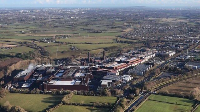
Fab 34 in Leixlip has long evolved beyond being just another corporate plant; today, it stands as Intel's strategic European stronghold. The facility possesses a critical competitive edge: the implementation of Extreme Ultraviolet (EUV) lithography, enabling transistor densities unattainable through traditional methods. In the current landscape, Fab 34 remains the company's sole site in Europe capable of mass-producing chips to the most advanced standards, rendering it a pivotal asset in Intel's global supply chain diversification strategy.
The next phase of the plant's evolution involves a €5 billion investment, earmarked not only for hardware procurement but for a comprehensive overhaul of internal infrastructure. A primary focus is being placed on cleanroom logistics. Intel plans to integrate all facility modules into a single intelligent network, deploying an automated wafer transport system via overhead rails. This optimization of material flow is critical for minimizing defects and maximizing line throughput, which will significantly scale production volumes for the Intel 3 process.
While the facility's current technical roadmap is centered on Intel 3, the long-term horizon points toward more radical shifts: the Intel 18A and 18A-P nodes. Entering the "Angstrom era" represents a quantum leap in transistor energy efficiency and performance. The modernization of Fab 34 is laying the groundwork for chips where feature sizes are measured not in nanometers, but in tenths of a nanometer, paving the way for fundamentally new computing architectures.
Within Intel's current manufacturing hierarchy, there is a clear delineation of roles between different process nodes. The Intel 3 technology serves as the baseline for creating I/O dies and foundational substrates, which are particularly critical for data center infrastructure. For instance, the compute cores in Xeon 6 processors (known as Granite Rapids) are manufactured to this standard. Conversely, more complex components—such as the compute tiles in the Clearwater Forest or Diamond Rapids series—are migrating to the Intel 18A process and its 18A-P variant. This hybrid approach optimizes production costs by reserving the most expensive, cutting-edge nodes exclusively for where peak performance is indispensable.
Intel is currently seeing a surge in demand for these so-called "base dies." While the primary consumer remains internal, growing interest from external clients validates the viability of the Intel Foundry Services (IFS) model. The company is effectively transforming into an open semiconductor manufacturer, poised to service third-party projects.
Despite these ambitions, Intel is exercising caution regarding further expansion in Europe. The construction of new plants has been paused until a "critical mass" of external clients is achieved. This is a pragmatic strategy: before committing tens of billions to new physical infrastructure, the corporation intends to ensure sustainable market demand and secure a pool of long-term contracts that justify scaling production across the European continent.
 The Strategic Alliance of Nvidia and MediaTek