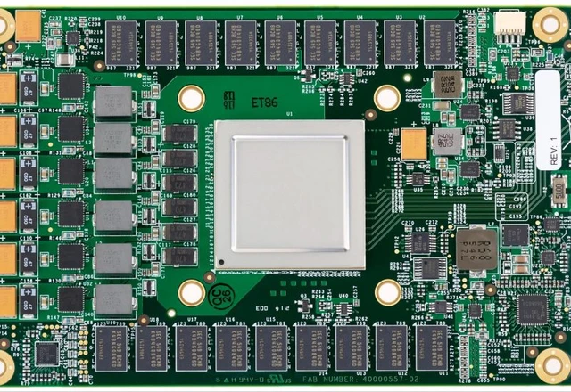
The global AI race is shifting from the realm of algorithms to the physical layer of hardware. As tech titans strive to decouple themselves from a systemic reliance on a single chip supplier, the very landscape of the semiconductor industry is being reshaped. Samsung Electronics is doubling down on the contract manufacturing of specialized integrated circuits, offering the market an unprecedented degree of vertical integration. Strategic alliances with Meta and Anthropic are positioning the Korean giant as the critical bedrock for the next generation of computational power.
The contemporary AI accelerator landscape has long been defined by a de facto monopoly, where access to critical compute resources was dictated by one's ability to secure hardware from a handful of dominant suppliers. However, the era of general-purpose solutions is drawing to a close. The prevailing trend is now a decisive shift toward ASICs (Application-Specific Integrated Circuits)—chips precision-engineered for the specific requirements of a particular neural network, allowing for exponential gains in both energy efficiency and raw performance.
Within this paradigm, Samsung Electronics is pivoting its business model, transforming its Foundry division into the primary manufacturing hub for the world's tech giants. Following a successful collaboration with Tesla, the company is aggressively expanding its roster of strategic partners to include Meta and Anthropic. This is more than a mere expansion of the client base; it is a transition toward a high-margin production model, with a mid-term order backlog projected to reach a staggering $32.74 billion.
A cornerstone of this strategy is the partnership with Meta. The social media giant is striving for complete computational sovereignty by developing its own MTIA accelerators. While the first two generations of these chips were produced via Taiwan's TSMC, the third generation will be built on Samsung's cutting-edge 2nm process node. Meta's ambitions extend far beyond a simple server refresh: the company plans to deploy a data center network with a total capacity of 5 GW by 2030. Furthermore, owning its own silicon paves the way for Meta to enter the Cloud Service Provider (CSP) market, where it could lease MTIA-powered compute capacity to third-party developers.
The pace of hardware iteration at Meta is approaching an assembly-line cadence, with the company intending to release a new iteration of accelerators every six months. Such an aggressive development cycle is impossible to sustain using in-house resources alone; consequently, Meta has fused its capabilities with Samsung’s System LSI division. This synergy allows for the integration of a deep understanding of AI workloads with world-class semiconductor engineering expertise.
Parallel to Meta, Anthropic is also integrating into the Samsung ecosystem. As one of the leading developers of Large Language Models (LLMs), Anthropic is similarly seeking to mitigate its reliance on Nvidia and Google by commissioning its own 2nm ASICs. The scale of Anthropic's planned infrastructure is immense: a proposed 1 GW data center project requires investments of approximately $50 billion, half of which will be allocated to chip procurement.
In this arena, Samsung is leveraging its primary competitive advantage: a holistic, integrated approach. Unlike specialized foundries, the Korean giant controls the entire value chain—from the design and fabrication of the logic dies (ASICs) to the production of high-speed DRAM and NAND flash storage, and finally, the advanced packaging. For Anthropic, this translates into a "turnkey solution" where memory and processing are perfectly synchronized for peak performance.
The strategic depth of these relationships is further evidenced by financial ties: Samsung has already participated as an investor in Anthropic's funding rounds, cementing the partnership with a formal agreement. In doing so, Samsung is evolving beyond the role of a contract manufacturer to become a true technological co-architect of the new AI era.

 The Price of Acceleration: CXMT’s Rapid Push into Memory