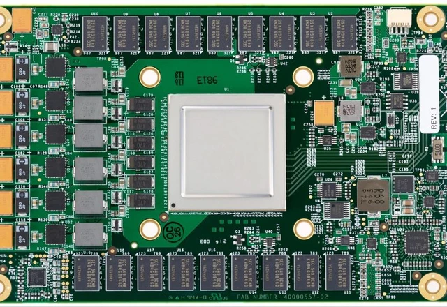
The race for nanometers has long since transcended marketing rhetoric, evolving into a high-stakes battle over fundamental power efficiency and transistor density. In the realm of mobile computing, the transition to a 2nm process is now viewed as the definitive gold standard for performance. Google sought to position itself at the vanguard of this technological sprint with its Pixel 11 lineup. However, reality has proven more pragmatic: the company has chosen a path of steady evolution over a radical leap forward.
In the semiconductor landscape, the battle is fought less over raw clock speeds and more over the physical scale of components. The transition from 3nm to 2nm is not merely a numerical adjustment in a spec sheet; it represents a qualitative leap in transistor architecture, enabling a radical reduction in power consumption while simultaneously boosting computational throughput. This is precisely why the industry has been watching with such intensity to see which tech giant would be the first to bring this standard to mass-market consumer devices.
Samsung has effectively claimed the first-mover advantage, introducing the Exynos 2600 chip built on a 2nm process. Against this backdrop, expectations for Google were exceptionally high: there was an anticipation that the Tensor G6 would be the catalyst allowing the Pixel 11 to leapfrog its competitors in both efficiency and hardware prestige.
However, Google’s strategy has proven more conservative. While the preceding Tensor G5 relied on a standard 3nm process, the new Tensor G6 remains within that same technological envelope. As confirmed by Vice President Peng Yu Chun, the chip utilizes an "enhanced" 3nm process. This indicates that engineers focused on optimizing existing manufacturing methods and refining the die architecture rather than migrating to a fundamentally new—and significantly riskier and more expensive—technological platform.
There are rational justifications for this approach. The shift to 2nm is fraught with immense challenges regarding yield rates and requires colossal capital investment in equipment. By choosing the path of optimization, Google minimizes the risks of defects and instability, though it forfeits a critical marketing advantage.
In contrast, the strategies of its competitors appear far more aggressive. Apple is expected to debut the iPhone 18 Pro powered by a full 2nm processor, allowing it to maintain its hegemony in energy efficiency. A similar trend is evident with Qualcomm; while official confirmation is pending, industry insiders suggest that future flagship Snapdragon solutions will also be based on 2nm.
Ultimately, Google finds itself facing a classic engineering trade-off: pushing the technological vanguard versus ensuring product stability. While the Tensor G6 may deliver respectable performance metrics, the absence of a move to 2nm strips the company of the opportunity to claim technological supremacy over Apple and Qualcomm at the very heart of mobile silicon.

 The Price of Acceleration: CXMT’s Rapid Push into Memory