The semiconductor industry has long been grappling with the physical limits of scaling traditional random-access memory. The quest to increase data density without compromising performance has evolved into the defining technological race of the decade. For years, SanDisk has been quietly developing 3D Matrix Memory, aiming to transpose the principles of vertical stacking—pioneered in NAND flash—into the realm of high-performance computing. Recent test results confirm that this conceptual framework is finally manifesting into a tangible physical reality.
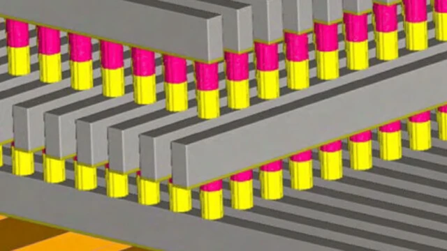
Modern DRAM has hit a ceiling where further process node shrinkage is no longer economically or technically viable. In this climate, vertical scaling has become the only logical path forward. The 3D Matrix Memory concept, which SanDisk has been developing since 2017, envisions a three-dimensional cell architecture designed to exponentially increase chip capacity while maintaining speeds comparable to traditional volatile memory.
A pivotal milestone in the latest development phase has been the successful fabrication of chips on standard 300mm wafers. This is a critical breakthrough: by utilizing industry-standard equipment, the technology avoids the need for entirely new fabrication plants and can instead be integrated into existing production cycles. Recent testing has confirmed the viability of individual memory segments with capacities of several gigabits, with performance metrics closely aligning with target specifications.
The development is being conducted in close collaboration with IMEC, the Belgian research hub and a global leader in new materials and lithography. These joint efforts have enabled a stacked memory layout across multiple levels, effectively transforming a flat data array into a multi-layered "metropolis" of cells. The ultimate goal of this ambitious project is to halve the cost per bit of information compared to current DRAM standards.
Despite this technical progress, the precise nature of the 3D Matrix Memory cell remains strictly classified. However, industry analysts point to two likely scenarios. The first is the use of Phase-Change Memory (PCM), where data is stored by switching the material between amorphous and crystalline states—an approach reminiscent of the 3D XPoint technology previously developed by SanDisk and Intel. The second possibility is ReRAM (Resistive RAM), which relies on altering the resistance of a dielectric. Given Western Digital's (SanDisk's parent company) experience with 4DS, this path also appears highly promising.
Nevertheless, the journey from laboratory prototype to mass-market product remains long. Company leadership has openly admitted that the project has a "long-term horizon," and concrete commercial launch dates have yet to be established. While previous roadmaps suggested chips with capacities of 32–64 Gb, the current focus has shifted toward ensuring the stability and reliability of these multi-layered structures.
The emergence of 3D Matrix Memory could fundamentally reshape the memory hierarchy of modern computing, collapsing the boundary between ultra-fast, expensive volatile memory and high-capacity, slower non-volatile storage. This would pave the way for entirely new classes of devices where massive datasets are accessible to the processor almost instantaneously.
 The Price of Acceleration: CXMT’s Rapid Push into Memory