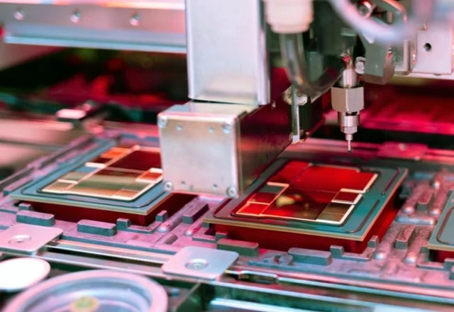
The pursuit of nanometer scaling has reached a critical juncture, where conventional EUV systems are no longer sufficient to drive further progress. Intel is now moving to break through this technological barrier by integrating High Numerical Aperture (High-NA) scanners directly into its manufacturing pipelines. This shift represents more than a mere technical upgrade; it is a strategic bet on the future scalability of semiconductor fabrication. The first real-world applications are already unfolding within the Panther Lake family of mobile processors.
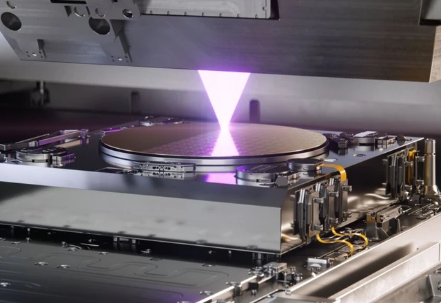
The modern microelectronics industry is currently navigating a volatile transition toward new methods of chip lithography. At the heart of this evolution lies Extreme Ultraviolet (EUV) technology, which has enabled the creation of transistors at an unprecedented scale. However, even EUV faces inherent resolution limits, forcing market leaders to seek greater precision. The solution is the shift toward High Numerical Aperture (High-NA) equipment, which allows for denser, sharper structures without the need for the cumbersome multi-patterning of a single layer.
Intel has begun the strategic integration of these systems into the production of its Panther Lake mobile processors. It is crucial to note that these chips are built on the Intel 18A process, which does not strictly mandate High-NA scanners to achieve its stated performance targets. Nevertheless, the company is consciously taking this step, treating the current production cycle as a large-scale proving ground for the hardware.
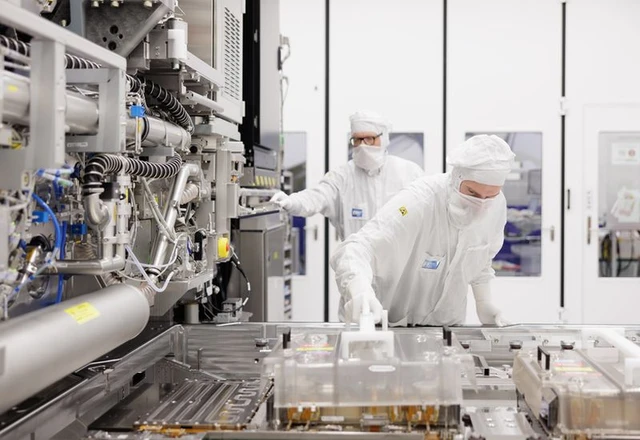
At this stage, the deployment of High-NA EUV is selective; the equipment is utilized only for the most critical and dense layers of the die. This approach allows Intel to accumulate vital practical expertise and optimize manufacturing processes in collaboration with ASML, all while mitigating risks to the overall wafer yield of the production batch.
The economic implications of this transition are staggering. With a single scanner costing upwards of $400 million, every technological decision becomes a high-stakes investment. For Intel, however, this strategy is justified by long-term objectives: the full transition to the 14A process, slated for 2027, will demand absolute mastery of High-NA tools, as alternatives at that level of precision virtually cease to exist.
In contrast, the stance of its primary competitor—Taiwan's TSMC—remains more conservative. Despite a keen interest in ASML’s latest capabilities, TSMC currently views the equipment costs as prohibitive for mass adoption. This creates a compelling market divergence: Intel is assuming the role of the pioneer and absorbing the primary financial risks, while TSMC prefers to wait for the technology to mature and costs to stabilize.
Ultimately, the use of High-NA in Panther Lake is less about immediate processor performance and more about laying the foundation for the next technological leap. Intel aims to transform theoretical lithographic possibilities into an industrial standard, securing its leadership in the era of sub-2nm silicon.
 The Horizon of China's Technological Sovereignty in Lithography