The global race for AI supremacy is no longer defined solely by the raw power of computing cores, but by the velocity of data exchange between them. High-bandwidth memory has emerged as the critical nexus—either unlocking new possibilities or imposing rigid constraints on the evolution of neural networks. In this climate, the move by Chinese player CXMT into the trial production phase of HBM3E marks a pivotal moment for the semiconductor industry. This is more than a simple portfolio expansion; it is a strategic bid to dismantle technological dependence on external suppliers.
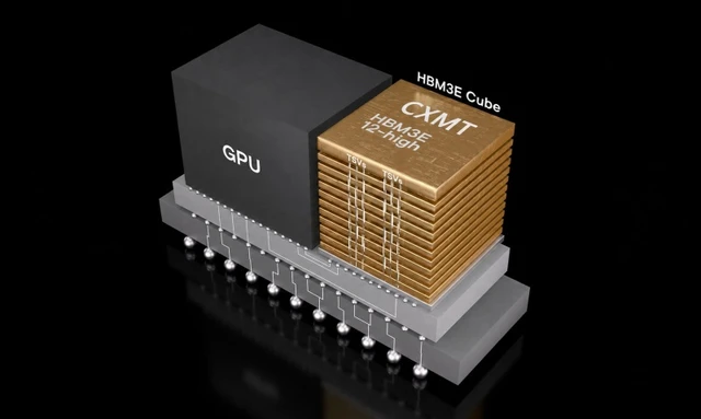
The contemporary high-performance computing (HPC) landscape demands massive data throughput coupled with minimal latency. This is precisely why High Bandwidth Memory (HBM) has become the gold standard for AI accelerators. In a strategic move to narrow the divide with global leaders, CXMT has begun producing test batches of HBM3E memory. These initial samples are already being integrated into the ecosystems of T-Head and Cambricon Technologies, signaling the emergence of a comprehensive end-to-end domestic development cycle—from memory die fabrication to integration into specialized processors.
Despite this progress, the reality on the ground is that Chinese manufacturers still lag behind South Korean giants like SK Hynix and Samsung by approximately two generations. While CXMT is mastering HBM3E, market leaders are already pivoting their capacities toward the HBM4E standard. However, CXMT's developmental trajectory is remarkable; the company is demonstrating an atypically aggressive pace of infrastructure deployment. The construction of cleanroom facilities, which typically takes up to two years in this industry, was completed in just 12 months—a testament to total resource mobilization and rigorous administrative oversight.
From a technical standpoint, the project's ambitions are clear. According to JEDEC specifications, HBM3E is characterized by a 1024-bit data bus width. Signal speeds per pin range from 9.2 to 12.4 Gbps, with a primary focus on a stable 9.6 Gbps. Collectively, this delivers a bandwidth of 1.2 TB/s, providing the necessary throughput to sustain the data-hungry requirements of the most demanding neural network models. Depending on the stack height—ranging from 8 to 12 layers—module capacities vary between 24 and 36 GB.
Scaling manufacturing has become the company's primary objective for the coming years. Currently, CXMT operates two 12-inch wafer fabrication plants in Hefei and Beijing, providing a total capacity of approximately 200,000 DRAM wafers per month. This is merely the opening gambit. By the end of the current year, capacity is expected to rise to 350,000 wafers, and with the full launch of new sites in Shanghai and Hefei, production capacity is projected to triple, reaching 600,000 wafers monthly.
By 2027, CXMT intends to fully operationalize the mass production of HBM3E, transitioning from pilot batches to a commercial-scale product. This trajectory reflects a broader trend toward the creation of a sovereign technology stack, where the speed of facility construction and aggressive volume scaling have become the primary levers for capturing market share in the era of Generative AI.
 The Korea-Japan Technological Alliance