The global semiconductor race is escalating into a phase of intense technological confrontation. Under the pressure of export restrictions imposed by the U.S. and the Netherlands, China is aggressively pursuing total autonomy in chip production. The development of indigenous Deep Ultraviolet (DUV) lithography systems has become a critical milestone in the quest to master 7-nanometer process nodes. This strategy will define not only the region's economic trajectory but also the global balance of power within the high-tech industry.
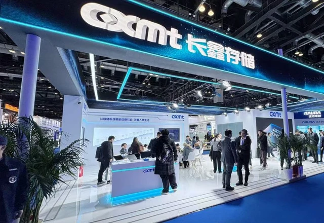
An ambitious initiative to establish a national lithography base is taking shape in Shanghai. A state-owned enterprise, whose identity remains undisclosed, has commenced the mass production of Deep Ultraviolet (DUV) immersion lithography systems. The first shipments are expected within the current year, with industry giants such as SMIC, Hua Hong Semiconductor, and memory manufacturer ChangXin Memory Technologies poised to be the primary beneficiaries.
The rollout strategy is cautious yet methodical: five units are slated for delivery by 2026, with that number projected to rise to twenty by 2027. This measured pace is dictated by the current geopolitical climate. The U.S. Congress is considering legislation that would effectively block Chinese semiconductor firms from collaborating with ASML—the world's sole provider of the most advanced lithography equipment. Consequently, domestic development has evolved from a matter of national prestige into an existential necessity for China's tech sector.
To achieve this goal, a powerhouse engineering hub is being assembled. The manufacturer is aggressively recruiting top-tier specialists from other Chinese entities, including the state-backed startup Shanghai Yuliangsheng Technology. The latter already plays a pivotal role in the ecosystem; SMIC is currently testing immersion systems from Yuliangsheng to evaluate the actual potential of domestic designs before they are deployed at scale.
However, the path toward total autonomy is fraught with technical hurdles. Despite a high degree of component localization, critical modules are still imported from Japan. Furthermore, delivery delays from local contractors have become the primary bottleneck limiting production volumes in the current period.
From a technical standpoint, utilizing DUV lithography to produce chips on a 7nm process is a complex compromise. While standard immersion technology allows for 28nm elements in a single exposure cycle, achieving 7nm requires multi-patterning. This method significantly increases the likelihood of overlay errors and inevitably leads to lower yields per wafer.
Against this backdrop, ASML’s dominance remains overwhelming. The company plans to ship approximately 130 immersion systems in 2026, demonstrating a scale of operations far beyond the reach of its Chinese counterparts. Moreover, the global market is steadily transitioning toward Extreme Ultraviolet (EUV) technology, which enables single-exposure patterning—a process that is both more cost-effective and efficient for producing modern DRAM and logic chips.
Analysts from the AI Futures Project remain conservative regarding the commercial viability of Chinese DUV lithography, forecasting a full market entry only by the mid-2030s. According to their data, ASML will continue to control over 98% of this segment. Currently, Chinese machines lag behind the original in terms of throughput and build quality, while EUV developments remain in the prototype stage, far from practical application in mass production.
Nevertheless, the shift toward the mass production of proprietary equipment signals Beijing's long-term strategy to break the technological blockade. Even with a significant gap between them and the market leaders, establishing its own lithography infrastructure allows China to mitigate the risks of sudden supply chain disruptions triggered by external sanctions.
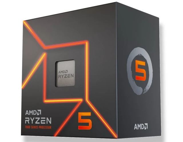 AMD’s Strategic Approach to the Budget Segment