The quest for novel materials has long been the primary bottleneck of technological advancement—a domain where theoretical predictions were frequently stifled by the sluggish pace of physical synthesis. While modern artificial intelligence can now architect structures with extraordinary properties, translating these digital blueprints into physical reality once demanded months of painstaking, manual labor. The emergence of specialized atomic printing platforms is shifting this paradigm, condensing the transition from hypothesis to tangible prototype into a matter of hours. The materials development cycle is now entering an era of total automation, positioning AI not merely as a tool, but as a fully autonomous chemical engineer.
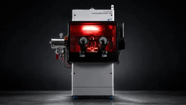
In modern materials science, a critical disconnect exists between digital simulation and physical experimentation. While machine learning algorithms propose thousands of candidates for new semiconductors or superconductors, chemists and physicists expend staggering resources on manual sample preparation. Enter the Nanofabricator Pro—a first-of-its-kind physical platform engineered for the direct implementation and validation of AI-proposed materials.
At the heart of the system lies Direct Atomic Layer Processing (DALP). To appreciate its significance, one must consider the traditional method of Atomic Layer Deposition (ALD). In conventional ALD, the chemical reaction blankets the entire substrate, necessitating subsequent photolithography—applying masks and etching away excess material to create the desired structures. DALP fundamentally disrupts this workflow. Instead of a uniform coating, it employs a miniature, mobile micro-reactor that confines the precursor interaction to a specific area of the surface.
Effectively, this transforms the synthesis process into high-precision "printing" guided by a digital blueprint. This enables the fabrication of structures with thickness control at the level of individual atomic layers, completely bypassing the photolithography stage. The system is compatible with over 450 material families, while software-driven control provides absolute flexibility in defining geometry, process parameters, and operational sequences.
However, the true value of the Nanofabricator Pro lies not merely in its printing precision, but in the creation of a closed-loop development cycle. In traditional workflows, any change in composition or deposition parameters requires a new wafer and a separate processing cycle. This new platform allows for the creation of numerous material combinations and structures on a single substrate.
This paves the way for the "autonomous laboratory" concept. The workflow is seamless: AI generates a hypothesis regarding material properties > the system synthesizes the sample > integrated metrology tools measure its characteristics > data is fed back into the algorithm to refine the model > a new, more accurate series of experiments is generated. This iterative cycle is critical for the development of quantum devices, advanced chip packaging, and next-generation semiconductors.
It is important to note that this technology is not intended to replace mass production. Its purpose is the radical acceleration of the R&D phase. The Nanofabricator Pro serves as a bridge, enabling the rapid identification of the optimal fabrication process before scaling it to an industrial level.
Looking ahead, such integration will lead to the creation of fully autonomous research centers. In these ecosystems, AI will do more than just suggest ideas; it will independently manage the realization process, conduct measurements, and correct its own errors, effectively reducing the time-to-discovery for new materials to an absolute minimum.
 Anthropic’s Strategic Push for Hardware Independence