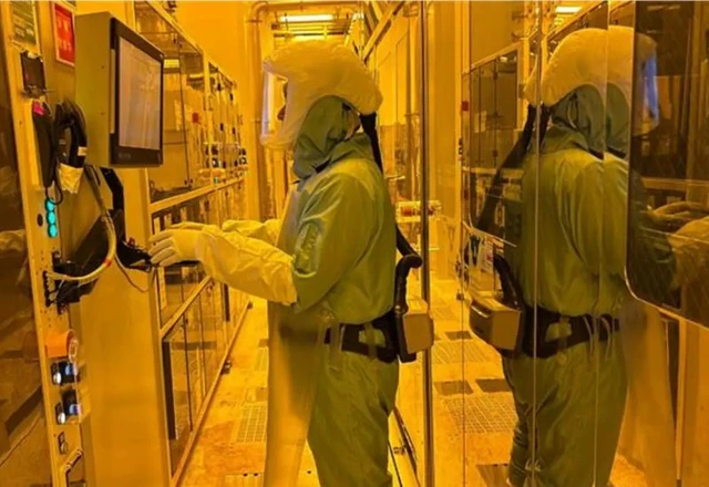
The modern semiconductor industry has evolved into a global race for nanometers, where every incremental gain defines the architecture of future computing systems. In this high-stakes competition, Taiwan's TSMC is seeking to cement its dominance by pivoting toward the A14 process node. This shift represents more than just the physical shrinking of transistors; it signals a radical transformation in industrial construction itself. The integration of artificial intelligence and virtual reality into fab deployment is becoming the new benchmark for efficiency, enabling the industry to bypass traditional temporal constraints.
Deep within Taiwan’s Central Science Park in Taichung, a project is unfolding that could fundamentally shift the balance of power in the microelectronics market. TSMC is currently constructing a new fabrication plant dedicated to the A14 process, utilizing a 1.4nm node. According to current data, the facility is slated for completion by April 2027—a timeline that appears ambitious even for an industry titan of this magnitude.
This accelerated pace has been made possible through the integration of cutting-edge digital management tools. TSMC has essentially transformed the construction site into a proving ground for its own proprietary technologies: artificial intelligence is deployed for intelligent monitoring and pattern recognition, minimizing human error in the oversight of complex engineering systems. Simultaneously, virtual reality is being leveraged for workforce training. VR simulations allow personnel to rehearse maneuvers in potentially hazardous scenarios and master working at height, drastically reducing onboarding time while elevating safety standards.
This synergistic approach to construction allows the company to significantly compress its schedule. The transition from groundbreaking to initial pilot production is expected to be completed by the end of 2027, with full-scale mass production of the A14 process scheduled for 2028.
From a technical standpoint, A14 represents an evolutionary leap over its predecessor, the N2 (2nm) node. In an era where Moore’s Law is colliding with the physical limitations of silicon, every incremental gain in efficiency becomes critical. The A14 process promises either a 15% boost in performance at current power levels or a 30% reduction in energy consumption while maintaining existing performance. Furthermore, logic density is increasing by 20%, and system scalability has become significantly more flexible than in any previous iteration.
The stakes of this race are strategic. Achieving mass production by 2028 will provide TSMC with a critical window of advantage over its primary rivals—Samsung and Intel—both of whom are pursuing nodes of similar scale. In a world where the demand for high-performance computing (HPC) to power AI is growing exponentially, even a few months' lead can translate into total market dominance over the planet's most advanced processors.
 Anthropic’s Strategic Financial Surge Ahead of Its IPO