The contemporary AI arms race has shifted its center of gravity, moving beyond algorithmic innovation into the realm of physical manufacturing. Today's critical bottlenecks are no longer confined to lithography alone; they now encompass the final stages of assembly and testing for these intricate systems. TSMC, the global industry titan, is addressing this challenge through a massive infrastructural expansion across Taiwan. These new advanced packaging facilities are designed to alleviate the shortage of high-performance accelerators—the very hardware defining the architecture of today's computing landscape.
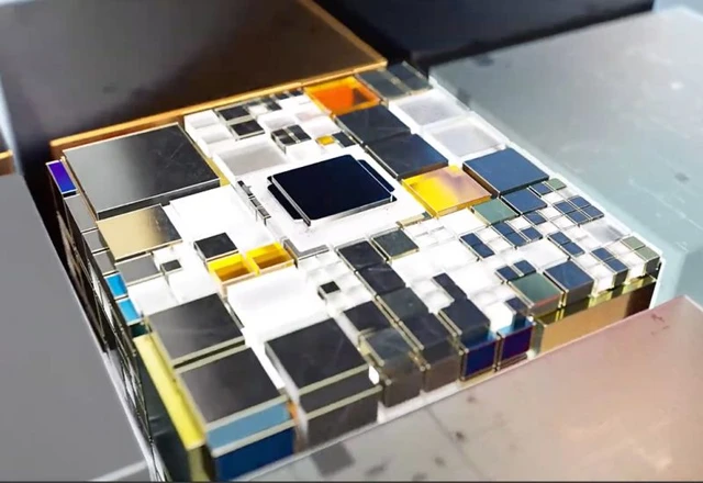
In the era of the meteoric rise of generative AI, the semiconductor industry has encountered a fundamental paradox: transistor density on silicon wafers is no longer the sole determinant of performance. The spotlight has shifted toward Advanced Packaging—the art of integrating multiple dies into a single, high-performance module. This shift is the primary driver behind TSMC’s massive capacity expansion across southern Taiwan.
The strategic epicenter of this expansion is the Chiayi Science Park. According to company blueprints, this region is slated to become the premier hub for the testing and packaging of the most sophisticated chips produced for TSMC's tier-one clients. This is not merely about constructing a single plant, but about fostering a comprehensive industrial cluster. The project envisions the commissioning of four specialized facilities; currently, the first has entered mass production, while the groundbreaking of the second facility officially marks the next phase of scaling.
It is critical to recognize that this expansion is dictated by acute market pressures. Industry titans such as Nvidia are grappling with a chronic shortage of AI accelerators. The crux of the problem is that even when lithography capacity is available, the final assembly process—specifically the use of CoWoS (Chip on Wafer on Substrate) technology to integrate logic chips with HBM (High Bandwidth Memory)—remains labor-intensive and slow. This stage has become the primary bottleneck stifling the growth of the entire neural network computing market.
The economic dividends of this strategy are poised to be immense. Preliminary estimates suggest that once all four facilities in the Chiayi Science Park are fully operational, the complex's aggregate annual revenue will exceed $9.35 billion. Beyond the financial metrics, the project is expected to create over 9,000 high-tech jobs, significantly bolstering the region's industrial potential.
Ultimately, TSMC is pivoting its business model, evolving from a pure-play wafer foundry into a comprehensive provider of system assembly solutions. As Moore's Law loses momentum, innovations in advanced packaging and 3D stacking have become the primary levers for scaling computational power, enabling the creation of devices that will fuel the next wave of the technological revolution.
 The Strategic Alliance of Nvidia and MediaTek