The global surge in AI demand is fundamentally reshaping the hardware requirements for computing systems. For years, China's memory market was largely confined to the role of a module assembler; however, we are now witnessing a fundamental pivot toward deep technological synthesis. The shift toward advanced chip packaging is proving critical in overcoming the physical constraints inherent in traditional semiconductors. Strategic investments by industry players like Biwin underscore the region's ambition to transcend mere assembly and carve out a dominant position in high-end technological design.
The era of commodity assembly—where SSDs were simply cobbled together from third-party components—is drawing to a close. China's memory market players have recognized that the strategic competitive edge no longer lies in production volume, but in the sophistication of chip packaging and testing. It is here, at the convergence of materials science and microelectronics, that the performance benchmarks for future systems are being defined.
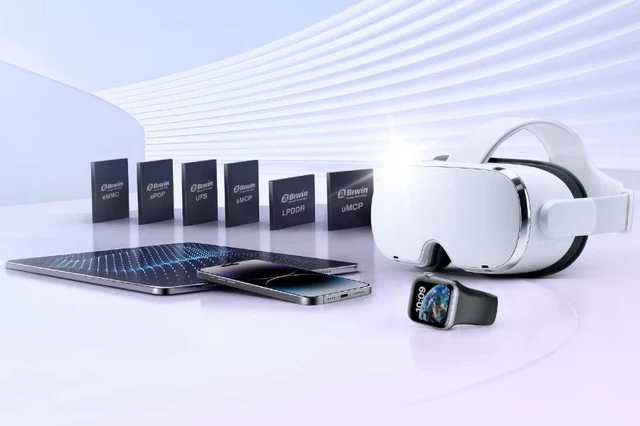
A prime example of this transformation is the strategy adopted by Biwin Storage Technology. The company has invested 4.5 billion yuan (approximately $672 million) into an ambitious initiative to implement advanced packaging methods in Dongguan. This is not a sporadic effort but a systemic evolution: the current stage is the third in a series of expansions, with previous phases requiring an additional 3.09 billion yuan. Although the facility has not yet reached the mass-market sales stage—focusing instead on sample delivery and process optimization—the company's ambitions are precise: by the end of 2027, production capacity is expected to more than triple, reaching 10,000 silicon wafers per month.
Biwin’s technological stack is evolving from traditional methods toward more complex architectural concepts. Central to this shift is fan-out technology, which enables the creation of multi-layer memory structures with higher interconnect density, bypassing the inherent limitations of classical substrates. In parallel, the company is mastering chiplet-based architectures, allowing up to ten functional units to be integrated into a single package. This approach enables the efficient pairing of memory and logic blocks, a critical requirement for modern accelerators. Furthermore, in collaboration with partners, the company is exploring the integration of optical components directly into the chip package, which could potentially eliminate the data transmission "bottleneck."
The drive toward technological sovereignty is extending to other industry players as well. Shenzhen Techwinsemi Technology has migrated critical die-testing processes to its own facilities, establishing the foundation for a vertically integrated production cycle. Meanwhile, Shenzhen Longsys Electronics has pivoted toward ultra-compact solutions. The company has deployed capacities to produce over one million miniature SSDs per month using System-in-Package (SiP) technology. Under this approach, the controller, flash memory, and power management modules are consolidated into a single hermetic package, significantly reducing the physical footprint in the new generation of AI PCs.
This shift in business models—from "procurement and assembly" to "design and packaging"—is dictated by the rigorous demands of the AI era. Modern high-performance computing (HPC) hardware requires more than just increased memory capacity; it demands a radical surge in throughput coupled with a simultaneous reduction in power consumption and physical dimensions. In this environment, packaging ceases to be a secondary step and becomes the defining factor in the reliability and efficiency of the entire device.
Market indicators underscore the scale of this trend. The global advanced chip packaging market, valued at $46.1 billion in 2024, is projected to grow to $79.4 billion by 2030. The primary driver of this growth is the synergy between artificial intelligence and high-performance computing, where traditional packaging methods can no longer sustain the workloads. Consequently, Chinese memory manufacturers are moving up the value chain, evolving from mere assemblers into full-fledged technological architects.
 Qualcomm’s New Standard for Mobile Performance