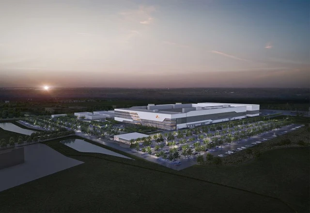
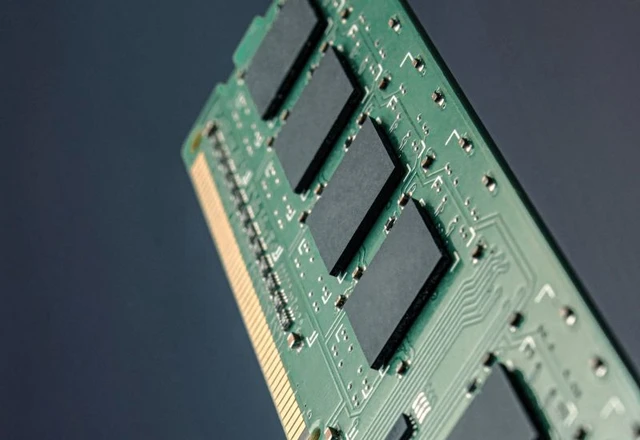
The global AI surge has triggered a tectonic shift in the semiconductor manufacturing landscape. A market that for decades operated on the basis of demand forecasting is rapidly evolving into a supply-constrained ecosystem. Industry titans such as Samsung and TSMC are now in a position to dictate new financial terms to their partners—a trend that underscores the critical dependency of the modern tech stack on a handful of concentrated manufacturing hubs.
The microelectronics industry has entered a period of rigorous resource cost reassessment. Samsung, one of the few global players capable of operating at nanometer scales, has announced a significant price hike for silicon wafers used in 4nm and 5nm process nodes. This increase of approximately 15% serves as a stark signal to all chip designers. Notably, this price correction has extended to less advanced segments—specifically certain 8nm automotive-grade chips—indicating capacity constraints even within specialized niches.
Historically, the synergy between fabless designers and foundries was built on deep partnerships and long-term strategic planning. Taiwan's TSMC, the sector's dominant leader, spent years cultivating relationships with giants like Apple, guided by demand forecasting. Major corporations essentially co-invested in the creation of new production lines to secure capacity ahead of flagship product launches. In this paradigm, the market remained fundamentally client-centric.
However, the meteoric rise of generative AI has fundamentally rewritten the rules of engagement. The surging demand for specialized accelerators, such as Nvidia's solutions, has transformed the semiconductor industry into a supplier-driven market. When the demand for compute power begins to exponentially exceed the physical capacity of fabs, the balance of power shifts toward the manufacturers. TSMC and Samsung are now in a position to hike prices, prioritizing clients willing to pay a premium for access to a limited supply of wafers.
This is a systemic shift. TSMC has similarly revised its pricing, increasing production costs by 5–10% for 3nm and 5nm processes, and even the more mature 7nm node. Consequently, rising costs have become an industry-wide trend, spanning a broad spectrum of cutting-edge technologies.
The situation is further compounded by the exponential rise in the cost of developing next-generation process nodes. The transition to 2nm nodes demands colossal investment in equipment—specifically Extreme Ultraviolet (EUV) lithography systems—and the development of novel materials. With orders from tech giants surging, manufacturers are seeking not only to recoup their R&D expenditures but to maximize profits during this period of acute scarcity.
Ultimately, these dynamics will drive up the cost of end-user devices and cloud computing services. The global reliance on a handful of fabrication sites in South Korea and Taiwan has transformed silicon access into a strategic resource—one whose value is no longer determined by market consensus, but by the physical limits of fab throughput.

 Nvidia’s Technological Pragmatism in the Open-Model Race