The race for compute density in data centers has entered a new, more aggressive chapter. Intel’s newly unveiled Diamond Rapids processor family marks a decisive pivot toward extreme chiplet integration. By synthesizing cutting-edge lithography with 3D packaging, Intel aims to redefine the very boundaries of server performance. This is far more than a mere iterative update; it is a fundamental paradigm shift in how silicon interacts with massive datasets.
The high-performance computing (HPC) landscape is on the cusp of a paradigm shift, and Xeon Diamond Rapids is positioned as the keystone of this transition. The primary technological breakthrough in these new chips is the implementation of the Intel 18A-P process—an enhanced iteration of the 18A node engineered specifically for the extreme optimization of transistor performance and power efficiency.
Intel’s engineering philosophy here is purely pragmatic: high-performance transistors now utilize dual power contacts on the backside of the die, radically improving power delivery. Furthermore, the threshold voltage (Vt) matrix has been expanded with the introduction of a fifth pair of options between the Low Voltage (LVT) and Ultra Low Voltage (ULVT) tiers. This allows for the granular tuning of every transistor, striking a precise balance between switching speeds and thermal output.
Particular emphasis has been placed on mitigating parameter variability. Intel has successfully achieved a 33% reduction in variance across PVT (Process, Voltage, Temperature) corners, which account for manufacturing deviations, voltage fluctuations, and thermal profiles. Consequently, transistors exhibit greater uniformity both within a single wafer and across different dies. For architects, this means the ability to tighten "guardbands" for clock frequencies and timings, directly resulting in higher operating frequencies, improved energy efficiency, and, crucially, an increase in die yield per wafer.
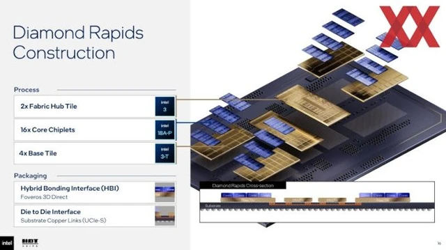
Structurally, Diamond Rapids is a sophisticated multi-layered "sandwich" of specialized chiplets. At the heart of the system lie two I/O Memory Hub (IMH) tiles, fabricated using the Intel 3 process, which handle all memory operations and external interfaces. Above them sit up to four Base Tiles (Intel 3-T), serving as the foundation and housing the Last Level Cache (LLC).
The top layer consists of the compute Core Tiles, manufactured using the cutting-edge 18A-P process. This is where the processor cores and their local L1 and L2 caches are concentrated. To integrate these layers, Intel employs Foveros 3D Direct packaging with a Hybrid Bonding Interface (HBI), minimizing latency during data transfer between the cores and the shared cache. Communication between the Base Tiles and the IMH hub is managed via a die-to-die (D2D) interconnect based on the UCIe-S standard.
The system's scalability is impressive: up to 16 compute Core Tiles can interface with the two central IMH hubs. Since each module contains 16 cores, the total core count per processor reaches 256. To feed this massive computational power, Intel has integrated a colossal amount of Last Level Cache—up to 1.28 GB (320 MB per each of the four Base Tiles), accessed via a high-speed 3D Xbar interconnect.
The memory and I/O subsystem has also received a significant upgrade. Each IMH Tile is equipped with six D2D PHYs and Unified Memory Fabric components, including memory controllers, snoop filters, and hardware encryption accelerators. Support for DDR5-12800 provides an aggregate bandwidth of up to 1.6 TB/s, while 128 PCI Express lanes allow for the connection of a vast array of peripherals and accelerators via CXL or UPI.
Beyond raw compute power in the form of cores and cache, Diamond Rapids is armed with a robust toolkit for AI and security. Support for AMX and AVX 10.2 instruction sets, alongside QAT, DSA, and IAA hardware accelerators, makes the processor a highly efficient tool for big data processing. Data protection is ensured by Intel TDX and SGX technologies, while overall system reliability is maintained through enhanced RAS (Reliability, Availability, and Serviceability) and QoS (Quality of Service) mechanisms—critical requirements for cloud infrastructure and enterprise data centers.
 The Economic Paradox of the GeForce RTX 5090