The global arms race for AI compute is shifting its focus from software optimization to the fundamental physics of semiconductors. The migration toward ultra-fine process nodes has become the sole viable path to achieving the transistor density and power efficiency required by next-generation autonomous systems. The newly forged alliance between Samsung and Tesla signals a strategic pivot in the manufacturing of bespoke accelerators; at the heart of this evolution lies the AI5 chip, engineered to serve as the bedrock for the next era of robotics and autonomous mobility.
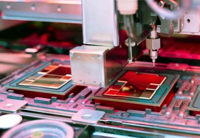
The semiconductor industry is entering an era of extreme miniaturization, where every single nanometer defines a product's competitive edge. Samsung Foundry is now commencing the mass production of Tesla’s specialized AI5 chips, leveraging a cutting-edge 2nm-class process. Production is centered at the Taylor plant, underscoring a strategic push to localize high-tech manufacturing and streamline logistics chains.
Tesla’s strategy here is rooted in risk mitigation: the AI5 is being manufactured concurrently across both Samsung and TSMC facilities. This dual-sourcing approach not only guarantees the volumes required for mass-market deployment but also fosters a healthy competitive tension between the world's two leading foundries.
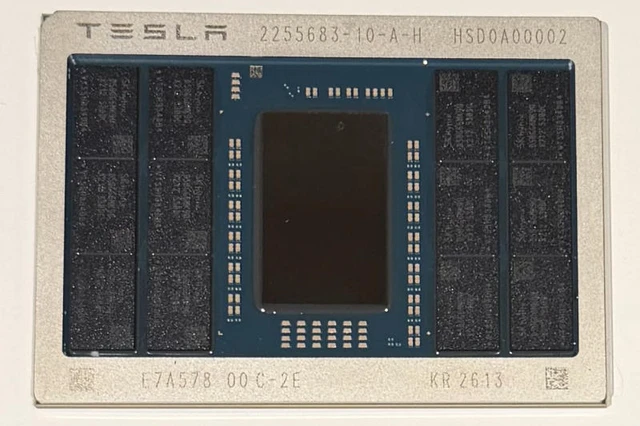
A technical analysis of the first AI5 sample reveals the developers' immense ambitions regarding data processing. The accelerator die is remarkably compact, occupying roughly half the reticle limit of a modern photolithography system. However, the system's true power resides in its memory subsystem. The integration of 12 SK hynix chips—likely GDDR6 or the latest GDDR7 standard—on an organic substrate indicates a concerted effort to dismantle the "memory wall" and eliminate bandwidth bottlenecks.
Assuming a bus width of 384 bits, the system is capable of delivering massive throughput, with estimates ranging from 768 GB/s to the terabyte scale. In the context of neural network computations, such bandwidth is critical for minimizing latency during the transfer of model weights and the real-time processing of sensor data.
The anticipated performance leap over the previous generation could be as high as 40x. Such a radical jump is made possible not only by the node shrink but also through the optimization of internal compute core architectures and the adoption of more efficient data interconnects.
The application spectrum for the AI5 extends far beyond the automotive sector. This chip is envisioned as a universal computing module for Tesla's entire ecosystem: from onboard computers in electric vehicles to humanoid robots and massive data centers used for neural network training. Consequently, the AI5 serves as the critical link between edge computing on devices and cloud infrastructure, creating a unified technological stack for the realization of full-scale artificial intelligence.
 The Horizon of China's Technological Sovereignty in Lithography